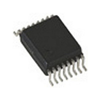
TDA5102NT Infineon Technologies, TDA5102NT Datasheet - Page 27

TDA5102NT
Manufacturer Part Number
TDA5102NT
Description
Manufacturer
Infineon Technologies
Datasheet
1.TDA5102NT.pdf
(35 pages)
Specifications of TDA5102NT
Operating Temperature (max)
85C
Operating Temperature Classification
Commercial
Product Depth (mm)
4.4mm
Operating Supply Voltage (min)
2.1V
Operating Supply Voltage (typ)
2.5/3.3V
Lead Free Status / Rohs Status
Not Compliant
Wireless Components
If the FSK switch is closed, Cv- is equal to Cv1 (C6 in the application diagram).
If the FSK switch is open, Cv2 (C7 in the application diagram) can be calculated.
Csw:
Remark:
2. Design hints on the buffered clock output (CLKOUT)
The CLKOUT pin is an open collector output. An external pull up resistor (RL)
should be connected between this pin and the positive supply voltage. The
value of RL is depending on the clock frequency and the load capacitance CLD
(PCB board plus input capacitance of the microcontroller). RL can be calculated
to:
Remark: To achieve a low current consumption and a low
Table 4-2
CLD
5
10
20
[
pF
]
parallel capacitance of the FSK switch (3 pF)
spurious radiation, the largest possible RL should be chosen.
These calculations are only approximations. The necessary values
depend on the layout also and must be adapted for the specific
application board.
fCLKOUT=
Cv
894 kHz
2
=
C
4 - 7
RL
RL
7
=
[
=
kOhm
6.8
27
12
Csw
fCLKOUT
∗
]
Cv
1
(
−
Cv
1
(
*
Cv
+
8
CLD
)
*
+
−
CLD
)
10
20
Cv
∗
5
[
(
pF
Cv
1
]
Specification, October 2001
1
fCLKOUT=
3.57 MHz
+
Csw
)
RL
Applications
TDA 5102
[
kOhm
6.8
3.3
1.8
]


