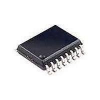
74LVC595APW NXP Semiconductors, 74LVC595APW Datasheet - Page 5

74LVC595APW
Manufacturer Part Number
74LVC595APW
Description
Counter Shift Registers 3.3V 8 SHIFT REG OTPT LATCH 3S
Manufacturer
NXP Semiconductors
Datasheet
1.74LVC595AD112.pdf
(19 pages)
Specifications of 74LVC595APW
Counting Sequence
Serial to Serial/Parallel
Number Of Circuits
1
Package / Case
SOT-403
Logic Family
LVC
Logic Type
CMOS
Output Type
3-State
Propagation Delay Time
4.7 ns, 4 ns
Supply Voltage (max)
3.6 V
Maximum Operating Temperature
+ 125 C
Minimum Operating Temperature
- 40 C
Function
Shift Register
Mounting Style
SMD/SMT
Operating Supply Voltage
1.8 V, 2.5 V, 3.3 V
Lead Free Status / Rohs Status
Details
Other names
74LVC595APW,112
NXP Semiconductors
7. Functional description
Table 3.
[1]
8. Limiting values
Table 4.
In accordance with the Absolute Maximum Rating System (IEC 60134). Voltages are referenced to GND (ground = 0 V).
[1]
[2]
74LVC595A_1
Product data sheet
Input
SHCP STCP OE
X
X
X
X
Symbol
V
I
V
I
V
I
I
I
T
P
IK
OK
O
CC
GND
stg
CC
I
O
tot
H = HIGH voltage state;
L = LOW voltage state;
X = don’t care;
NC = no change;
Z = high-impedance OFF-state.
The input and output voltage ratings may be exceeded if the input and output current ratings are observed.
For SO16 packages: above 70 C the value of P
For TSSOP16 packages: above 60 C the value of P
For DHVQFN16 packages: above 60 C the value of P
= LOW-to-HIGH transition;
X
X
X
Function table
Limiting values
Parameter
supply voltage
input clamping current
input voltage
output clamping current
output voltage
output current
supply current
ground current
storage temperature
total power dissipation
L
L
H
L
L
L
MR
L
L
L
H
H
H
[1]
DS
X
X
X
H
X
X
Output
Q7S
L
L
L
Q6S
NC
Q6S
tot
Conditions
V
V
3-state
output HIGH or LOW state
V
T
Qn
NC
L
Z
NC
QnS
QnS
derates linearly with 8 mW/K.
amb
I
O
O
< 0 V
tot
Rev. 01 — 29 May 2007
> V
= 0 V to V
tot
derates linearly with 5.5 mW/K.
8-bit serial-in/serial-out or parallel-out shift register; 3-state
= 40 C to +125 C
derates linearly with 4.5 mW/K.
CC
Function
a LOW-state on MR only affects the shift register
empty shift register loaded into storage register
shift register clear; parallel outputs in high impedance OFF-state
logic HIGH-state shifted into shift register stage 0. Contents of all
shift register stages shifted through, e.g. previous state of stage 6
(internal Q6S) appears on the serial output (Q7S).
contents of shift register stages (internal QnS) are transferred to
the storage register and parallel output stages
contents of shift register shifted through; previous contents of the
shift register is transferred to the storage register and the parallel
output stages
or V
CC
O
< 0 V
[1]
[1]
[1]
[2]
Min
-
-
-
-
0.5
50
0.5
0.5
0.5
100
65
74LVC595A
Max
+6.5
-
+6.5
6.5
V
100
-
+150
500
50
50
CC
© NXP B.V. 2007. All rights reserved.
+ 0.5
Unit
V
mA
V
mA
V
V
mA
mA
mA
mW
C
5 of 19


