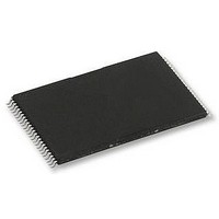
H27UAG8T2ATR-BC HYNIX SEMICONDUCTOR, H27UAG8T2ATR-BC Datasheet - Page 50

H27UAG8T2ATR-BC
Manufacturer Part Number
H27UAG8T2ATR-BC
Description
58T1891
Manufacturer
HYNIX SEMICONDUCTOR
Datasheet
1.H27UAG8T2ATR-BC.pdf
(61 pages)
Specifications of H27UAG8T2ATR-BC
Memory Type
Flash - NAND
Memory Size
16Gbit
Memory Configuration
2048M X 8
Supply Voltage Range
2.7V To 3.6V
Memory Case Style
TSOP
No. Of Pins
48
Operating Temperature Range
0°C To +70°C
Rohs Compliant
Yes
Available stocks
Company
Part Number
Manufacturer
Quantity
Price
Company:
Part Number:
H27UAG8T2ATR-BC
Manufacturer:
HYNIX
Quantity:
2 526
Company:
Part Number:
H27UAG8T2ATR-BC
Manufacturer:
SIEMENS
Quantity:
390
Company:
Part Number:
H27UAG8T2ATR-BC
Manufacturer:
HYNIX
Quantity:
4 000
Part Number:
H27UAG8T2ATR-BC
Manufacturer:
HYNIX/海力士
Quantity:
20 000
Rev 1.0 / Aug. 2010
tem controller can detect the completion of an erase by monitoring the R/B# output, or the Status bit (I/O 6) of the
Status Register. Only the Read Status command and Reset command are valid while erasing is in progress. When the
erase operation is completed, the Write Status Bit (I/O 0) may be checked. Figure 48 details the sequence.
4.14. Multi Plane Block Erase
Multiple plane erase, allows parallel erase of two blocks, one per each memory plane.
Block erase setup command (60h) must be repeated two times, each time followed by first block and second block
address respectively (3 cycles each). As for block erase, D0h command makes embedded operation start. Multi plane
erase does not need any Dummy Busy Time between first and second block address insertion. Address limitation
required for Multiple Plane Program applies also to multiple plane erase, as well as operation progress can be checked
like for Multiple Plane Program. Refer to the detail sequence as shown below.
4.15. Reset
The device offers a reset feature, executed by writing FFh to the command register. When the device is in Busy state
during random read, program or erase mode, the reset operation will abort these operations. The contents of memory
cells being altered are no longer valid, as the data will be partially programmed or erased. The command register is
cleared to wait for the next command, and the Status Register is cleared to value E0h when WP# is high. Refer to 2.8.
Status Register Coding for device status after reset operation. If the device is already in reset state, the command reg-
ister will not accept a new reset command. The R/B# pin goes low for t
to Figure 50.
■
■ Figure 49. Multi plane Block Erase
Figure 48. Block Erase
I/Ox
R/B#
R/B#
I/Ox
60h
Page address : Fixed “Low”
Plane address : Fixed “Low”
Block address : Block N
60h
Address
(3 cycle)
Row Add 1,2,3
Address
(3 cycle)
60h
D0h
Page address : Fixed “Low”
Plane address : Fixed “High”
Block address : Block M
Address
(3 cycle)
D0h
t
BERS
16Gb (2048M x 8bit) NAND Flash
RST
after the Reset command is written. Refer
t
BERS
70h
H27UAG8T2B Series
Status
70h
Status
Release
50


