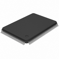
MAX4356ECD+T Maxim Integrated Products, MAX4356ECD+T Datasheet - Page 30

MAX4356ECD+T
Manufacturer Part Number
MAX4356ECD+T
Description
IC VIDEO CROSSPOINT SWIT 128TQFP
Manufacturer
Maxim Integrated Products
Datasheet
1.MAX4356ECD.pdf
(41 pages)
Specifications of MAX4356ECD+T
Function
Video Crosspoint Switch
Circuit
1 x 16:16
Voltage Supply Source
Single, Dual Supply
Voltage - Supply, Single/dual (±)
5V, ± 3 V ~ 5 V
Operating Temperature
-40°C ~ 85°C
Mounting Type
Surface Mount
Package / Case
128-TQFP, 128-VQFP
Lead Free Status / RoHS Status
Lead free / RoHS Compliant
16 x 16 Nonblocking Video Crosspoint Switch
with On-Screen Display Insertion and I/O Buffers
Intended for on-screen display insertion, the 16 OSD-
FILL inputs are buffered analog signal inputs that are
routed exclusively to a dedicated output buffer through
a fast 2:1 Mux. The signal presented to the output
buffer is selected from the programmed analog input
signal (IN_) and the dedicated OSDFILL input signal.
Each OSD Insertion Mux is controlled through the cor-
responding OSDKEY digital input to provide fast pixel
switching.
The MAX4356 has 256 individual T-switches making a
16 x 16 switch matrix . The switching matrix is 100%
nonblocking, which means that any input may be rout-
ed to any output. The switch matrix programming is
output-referred. Each output may be connected to any
one of the 16 analog inputs. Any one input can be rout-
ed to all 16 outputs with no signal degradation.
Table 1. Operation Truth Table
30
CE
X
1
0
0
0
0
______________________________________________________________________________________
UPDATE
X
X
1
0
1
0
OSDFILL and OSDKEY Inputs
SCLK
X
X
X
X
DIN
D
D
D
X
X
X
i
i
i
Switch Matrix
DOUT
D
D
D
X
i-96
X
X
i
i
MODE
X
1
1
0
0
X
AOUT
The digital interface consists of the following pins: DIN,
DOUT, SCLK, AOUT, UPDATE, CE, A3–A0, MODE, and
RESET. DIN is the serial data input; DOUT is the serial
data output. SCLK is the serial data clock that clocks
data into the Data Input registers (Figure 2). Data at
DIN is loaded at each falling edge of SCLK. DOUT is
the data shifted out of the 96-bit Complete Matrix Mode
(Mode = 1). DIN passes directly to DOUT when in
Individual Output Address Mode (Mode = 0).
The falling edge of UPDATE latches the data and pro-
grams the matrix. When using individual output
address mode, the address recognition output AOUT
drives low when control word bits D13 to D10 match
the address programming inputs (A3–A0) and UPDATE
is low. Table 1 is the operation truth table.
The MAX4356 offers two programming modes: individ-
ual output address mode and complete matrix mode.
X
1
1
1
0
X
RESET
1
1
1
1
1
0
No change in logic.
Data at DIN is clocked on the negative
edge of the SCLK into the 96-bit
Complete Matrix Mode register. DOUT
supplies original data in 96 SCLK
pulses later.
Data in the serial 96-bit Complete
Matrix Mode register is transferred
into parallel latches that control the
switching matrix.
Data at DIN is routed to the Individual
Output Address Mode shift register.
DIN is also connected directly to
DOUT so that all devices on the serial
bus may be addressed in parallel.
The 4-bit chip address A
compared to D
remaining 10 bits in the Individual
Output Address Mode register are
decoded, allowing reprogramming for
a single output. AOUT signals a
successful individual matrix update.
Asynchronous reset. All outputs are
disabled. Other logic remains
unchanged.
Programming the Matrix
OPERATION/COMMENTS
13
Digital Interface
to D
10
. If equal, the
3
to A
0
is


