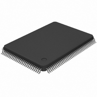
MAX4356ECD+T Maxim Integrated Products, MAX4356ECD+T Datasheet - Page 31

MAX4356ECD+T
Manufacturer Part Number
MAX4356ECD+T
Description
IC VIDEO CROSSPOINT SWIT 128TQFP
Manufacturer
Maxim Integrated Products
Datasheet
1.MAX4356ECD.pdf
(41 pages)
Specifications of MAX4356ECD+T
Function
Video Crosspoint Switch
Circuit
1 x 16:16
Voltage Supply Source
Single, Dual Supply
Voltage - Supply, Single/dual (±)
5V, ± 3 V ~ 5 V
Operating Temperature
-40°C ~ 85°C
Mounting Type
Surface Mount
Package / Case
128-TQFP, 128-VQFP
Lead Free Status / RoHS Status
Lead free / RoHS Compliant
Table 2. 16-Bit Serial Control Word Bit
Assignments (Mode 0: Individual Output
Address Mode)
These two distinct programming modes are selected
by toggling a single MODE pin high or low. Both modes
operate with the same physical board layout. This flexi-
bility allows initial programming of the IC by daisy-
chaining and sending one long data word while still
being able to address immediately and update individ-
ual outputs in the matrix.
Drive MODE to logic low to select mode 0. Individual
outputs are programmed through the serial interface
with a single 16-bit control word. The control word con-
sists of two don’t care MSBs, the chip address bits, out-
put address bits, an output enable/disable bit, an
with On-Screen Display Insertion and I/O Buffers
(MSB)
(LSB)
BIT
10
11
12
13
14
15
0
1
2
3
4
5
6
7
8
9
Individual Output Address Mode (MODE = 0)
16 x 16 Nonblocking Video Crosspoint Switch
Input Address 0
Input Address 1
Input Address 2
Input Address 3
Gain Set
Output Enable
Output Address B0
Output Address B1
Output Address B2
Output Address B3
IC Address A0
IC Address A1
IC Address A2
IC Address A3
X
X
NAME
______________________________________________________________________________________
LSB of input channel
select address
MSB of input channel
select address
Gain Select for output
buffer, 0 = gain of +1V/V,
1 = gain of +2V/V
Enable bit for output, 0 =
disable, 1 = enable
LSB of output buffer
address
MSB of output buffer
address
LSB of selected chip
address
MSB of selected chip
address
Don’t care
Don’t care
FUNCTION
output gain-set bit, and input address bits (Tables 2
through 6, and Figure 2).
In mode 0, data at DIN passes directly to DOUT
through the data routing gate (Figure 3). In this configu-
ration, the 16-bit control word is simultaneously sent to
all chips in an array of up to 16 addresses.
Drive MODE to logic high to select mode 1. A single
96-bit control word consisting of 16 six-bit control
words programs all outputs. The 96-bit control word’s
first 6-bit control word (MSBs) programs output 15, and
the last 6-bit control word (LSBs) programs output 0
(Table 7 and Figures 4 and 5). Data clocked into the
96-bit Complete Matrix Mode register is latched on the
falling edge of UPDATE, and the outputs are immedi-
ately updated.
The Complete Matrix Mode (Mode = 1) is convenient to
use to program the matrix at power-up. In a large
matrix consisting of many MAX4356 devices, all the
devices can be programmed by sending a single-bit
Table 3. Chip Address Programming for
16-Bit Control Word (Mode 0: Individual
Output Address Mode)
(MSB)
A3
0
0
0
0
0
0
0
0
1
1
1
1
1
1
1
1
IC ADDRESS BIT
A2
0
0
0
0
1
1
1
1
0
0
0
0
1
1
1
1
A1
0
0
1
1
0
0
1
1
0
0
1
1
0
0
1
1
Complete Matrix Mode (MODE = 1)
(LSB)
A0
0
1
0
1
0
1
0
1
0
1
0
1
0
1
0
1
ADDRESS
(HEX)
CHIP
Ch
Dh
Ah
Bh
Eh
0h
1h
2h
3h
4h
5h
6h
7h
8h
9h
Fh
Initialization String
ADDRESS
(DECIMAL)
ADDRESS
CHIP
10
11
12
13
14
15
0
1
2
3
4
5
6
7
8
9
31


