ADG784BCP-REEL Analog Devices Inc, ADG784BCP-REEL Datasheet

IC MUX/DEMUX QUAD 2X1 20LFCSP

ADG784BCP-REEL

Manufacturer Part Number
ADG784BCP-REEL
Description
IC MUX/DEMUX QUAD 2X1 20LFCSP
Manufacturer
Analog Devices Inc
Datasheet

Specifications of ADG784BCP-REEL

Rohs Status
RoHS non-compliant
Function
Multiplexer/Demultiplexer
Circuit
4 x 2:1
On-state Resistance
5 Ohm
Voltage Supply Source
Single Supply
Voltage - Supply, Single/dual (±)
1.8 V ~ 5.5 V
Current - Supply
1µA
Operating Temperature
-40°C ~ 85°C
Mounting Type
Surface Mount
Package / Case
20-VFQFN, CSP Exposed Pad
a
GENERAL DESCRIPTION
The ADG784 is a monolithic CMOS device comprising four
2:1 multiplexer/demultiplexers with high impedance outputs.
The CMOS process provides low power dissipation yet gives
high switching speed and low on resistance. The on-resistance
variation is typically less than 0.5 Ω with an input signal ranging
from 0 V to 5 V.
The bandwidth of the ADG784 is greater than 200 MHz and
this, coupled with low distortion (typically 0.5%), makes the
part suitable for switching fast ethernet signals.
The on-resistance profile is very flat over the full analog input
range ensuring excellent linearity and low distortion when switch-
ing audio signals. Fast switching speed, coupled with high signal
bandwidth, also makes the parts suitable for video signal switch-
ing. CMOS construction ensures ultralow power dissipation
making the parts ideally suited for portable and battery powered
instruments.
The ADG784 operates from a single 3.3 V/5 V supply and is
TTL logic compatible. The control logic for each switch is shown
in the Truth Table.
CMOS 3 V/5 V, Wide Bandwidth Quad 2:1
These switches conduct equally well in both directions when
ON, and have an input signal range that extends to the sup-
plies. In the OFF condition, signal levels up to the supplies
are blocked. The ADG784 switches exhibit break-before-
make switching action.
PRODUCT HIGHLIGHTS
1. Also Available as ADG774 in 16-Lead QSOP and SOIC.
2. Wide Bandwidth Data Rates >200 MHz.
3. Ultralow Power Dissipation.
4. Extended Signal Range.
5. Low Leakage over Temperature.
6. Break-Before-Make Switching.
7. Crosstalk is typically –70 dB @ 30 MHz.
8. Off isolation is typically –60 dB @ 10 MHz.
9. Available in Chip Scale Package (CSP).
The ADG784 is fabricated on a CMOS process giving an
increased signal range that fully extends to the supply rails.
This prevents channel shorting when the switches are config-
ured as a multiplexer.
Mux in Chip Scale Package
FUNCTIONAL BLOCK DIAGRAM
S1A
S1B
S2A
S2B
S3A
S3B
S4A
S4B
EN
DECODER
ADG784
1-OF-2
IN
ADG784
D1
D2
D3
D4

Related parts for ADG784BCP-REEL

ADG784BCP-REEL Summary of contents

Page 1

GENERAL DESCRIPTION The ADG784 is a monolithic CMOS device comprising four 2:1 multiplexer/demultiplexers with high impedance outputs. The CMOS process provides low power dissipation yet gives high switching speed and low on resistance. The on-resistance variation is typically less ...

Page 2

ADG784–SPECIFICATIONS SINGLE SUPPLY ( 10%, GND = 0 V. All specifications T DD Parameter ANALOG SWITCH Analog Signal Range On Resistance ( Resistance Match Between Channels (∆ Resistance Flatness (R ) ...

Page 3

SINGLE SUPPLY ( 10%, GND = 0 V. All specifications T DD Parameter ANALOG SWITCH Analog Signal Range On Resistance ( Resistance Match Between Channels (∆ Resistance Flatness (R ) FLAT(ON) ...

Page 4

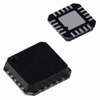
... S2B CONNECT NOTE: EXPOSED PAD TIED TO SUBSTRATE, GND. Model Temperature Range ADG784BCP –40°C to +85°C CAUTION ESD (electrostatic discharge) sensitive device. Electrostatic charges as high as 4000 V readily accumulate on the human body and test equipment and can discharge without detection. Although the ADG784 features proprietary ESD protection circuitry, permanent damage may occur on devices subjected to high-energy electrostatic discharges ...

Page 5

T 4 2.7V DD 4.0 3.5 3 3. 4.5V DD 2.0 1 5.0V DD 1.0 0.5 0 1.3 2.5 3 DRAIN OR SOURCE VOLTAGE – V ...

Page 6

ADG784 –5 –10 0 0.5 1.0 1.5 2.0 2.5 3.0 SOURCE VOLTAGE – BASE TX+ 10 BASE TX– 100 BASE TX+ 100 BASE TX– ...

Page 7

Test Circuits V1 0 0.1 F S1A S1B 0.1 F ADG784 S1A GND ...

Page 8

ADG784 R S S1A S1B V S S2A S2B S3A S3B S4A S4B PIN 1 INDICATOR 0.035 (0.90) MAX 0.033 (0.85) NOM SEATING PLANE V DD 0.1 F ADG784 S2A S1A GND 5V ...

Related keywords