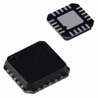
ADG784BCP-REEL Analog Devices Inc, ADG784BCP-REEL Datasheet - Page 4

ADG784BCP-REEL
Manufacturer Part Number
ADG784BCP-REEL
Description
IC MUX/DEMUX QUAD 2X1 20LFCSP
Manufacturer
Analog Devices Inc
Datasheet
1.ADG784BCPZ-REEL.pdf
(8 pages)
Specifications of ADG784BCP-REEL
Rohs Status
RoHS non-compliant
Function
Multiplexer/Demultiplexer
Circuit
4 x 2:1
On-state Resistance
5 Ohm
Voltage Supply Source
Single Supply
Voltage - Supply, Single/dual (±)
1.8 V ~ 5.5 V
Current - Supply
1µA
Operating Temperature
-40°C ~ 85°C
Mounting Type
Surface Mount
Package / Case
20-VFQFN, CSP Exposed Pad
ABSOLUTE MAXIMUM RATINGS
(T
V
Analog, Digital Inputs
Continuous Current, S or D . . . . . . . . . . . . . . . . . . . . 100 mA
Peak Current, S or D . . . . . . . . . . . . . . . . . . . . . . . . . . 300 mA
Operating Temperature Range
Storage Temperature Range . . . . . . . . . . . . –65°C to +150°C
Junction Temperature . . . . . . . . . . . . . . . . . . . . . . . . . . 150°C
Chip Scale Package
Lead Temperature, Soldering
ESD . . . . . . . . . . . . . . . . . . . . . . . . . . . . . . . . . . . . . . . . . 2 kV
NOTES
1
2
ADG784
CAUTION
ESD (electrostatic discharge) sensitive device. Electrostatic charges as high as 4000 V readily
accumulate on the human body and test equipment and can discharge without detection. Although
the ADG784 features proprietary ESD protection circuitry, permanent damage may occur on
devices subjected to high-energy electrostatic discharges. Therefore, proper ESD precautions are
recommended to avoid performance degradation or loss of functionality.
Model
ADG784BCP
Stresses above those listed under Absolute Maximum Ratings may cause perma-
Overvoltages at IN, S or D will be clamped by internal diodes. Current should be
nent damage to the device. This is a stress rating only; functional operation of the
device at these or any other conditions above those listed in the operational
sections of this specification is not implied. Exposure to absolute maximum rating
conditions for extended periods may affect device reliability. Only one absolute
maximum rating may be applied at any one time.
limited to the maximum ratings given.
DD
A
Industrial (B Version) . . . . . . . . . . . . . . . . –40°C to +85°C
θ
Vapor Phase (60 sec) . . . . . . . . . . . . . . . . . . . . . . . . . 215°C
Infrared (15 sec) . . . . . . . . . . . . . . . . . . . . . . . . . . . . . 220°C
= 25°C unless otherwise noted.)
JA
to GND . . . . . . . . . . . . . . . . . . . . . . . . . . –0.3 V to +6 V
Thermal Impedance . . . . . . . . . . . . . . . . . . . . . . 32°C/W
NC = NO CONNECT
NOTE: EXPOSED PAD TIED TO SUBSTRATE, GND.
S1A 1
S1B 2
S2A 4
S2B 5
PIN CONFIGURATION
D1 3
2
. . . . . . . . . . –0.3 V to V
(Pulsed at 1 ms, 10% Duty Cycle max)
ADG784
TOP VIEW
PIN 1
INDICATOR
30 mA, Whichever Occurs First
–40°C to +85°C
Temperature Range
1
15 S4A
14 S4B
13 D4
12 S3A
11 S3B
DD
+ 0.3 V or
ORDERING GUIDE
V
GND
S
D
IN
EN
R
∆R
R
I
I
I
V
C
C
C
t
t
t
Crosstalk
Off Isolation A measure of unwanted signal coupling through an
Bandwidth
Distortion
S
D
D
ON
OFF
D
DD
ON
FLAT(ON)
D
S
D
D
, I
(OFF)
Package Description
Chip Scale Package
(OFF)
ON
, C
(OFF)
(V
(OFF)
S
(ON)
S
S
)
(ON) “ON” Switch Capacitance.
Most Positive Power Supply Potential.
Ground (0 V) Reference.
Source Terminal. May be an input or output.
Drain Terminal. May be an input or output.
Logic Control Input.
Logic Control Input.
Ohmic resistance between D and S.
On Resistance match between any two channels
i.e., R
Flatness is defined as the difference between
the maximum and minimum value of on resis-
tance as measured over the specified analog
signal range.
Source Leakage Current with the switch “OFF.”
Drain Leakage Current with the switch “OFF.”
Channel Leakage Current with the switch “ON.”
Analog Voltage on Terminals D, S.
“OFF” Switch Source Capacitance.
“OFF” Switch Drain Capacitance.
Delay between applying the digital control input
and the output switching on. See Test Circuit 4.
Delay between applying the digital control input
and the output switching Off.
“OFF” time or “ON” time measured between
the 90% points of both switches, when switching
from one address state to another. See Test
Circuit 5.
A measure of unwanted signal that is coupled
through from one channel to another as a result
of parasitic capacitance.
“OFF” switch.
Frequency response of the switch in the ON
state measured at 3 dB down.
R
FLAT(ON)
ON
TERMINOLOGY
max – R
/R
L
ON
WARNING!
min.
ESD SENSITIVE DEVICE
Package Option
CP-20


