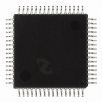
CLC018AJVJQ/NOPB National Semiconductor, CLC018AJVJQ/NOPB Datasheet - Page 3

CLC018AJVJQ/NOPB
Manufacturer Part Number
CLC018AJVJQ/NOPB
Description
IC CROSSPOINT SWITCH 8X8 64PQFP
Manufacturer
National Semiconductor
Datasheet
1.CLC018AJVJQNOPB.pdf
(17 pages)
Specifications of CLC018AJVJQ/NOPB
Function
Crosspoint Switch
Circuit
1 x 8:8
Voltage Supply Source
Dual Supply
Voltage - Supply, Single/dual (±)
±4.5 V ~ 5.5 V
Operating Temperature
-40°C ~ 85°C
Mounting Type
Surface Mount
Package / Case
64-QFP
Lead Free Status / RoHS Status
Lead free / RoHS Compliant
Other names
*CLC018AJVJQ
*CLC018AJVJQ/NOPB
CLC018AJVJQ
*CLC018AJVJQ/NOPB
CLC018AJVJQ
Available stocks
Company
Part Number
Manufacturer
Quantity
Price
Company:
Part Number:
CLC018AJVJQ/NOPB
Manufacturer:
IDT
Quantity:
300
Company:
Part Number:
CLC018AJVJQ/NOPB
Manufacturer:
Texas Instruments
Quantity:
10 000
Control Inputs:
MISCELLANEOUS PERFORMANCE
V
V
V
V
Input Capacitance
Output Capacitance
Electrical Characteristics
CC
CC
LL
LL
(V
Note 1: “Absolute Maximum Ratings” are those values beyond which the safety of the device cannot be guaranteed. They are not meant to imply that the devices
should be operated at these limits. The table of “Electrical Characteristics” specifies conditions of device operation.
Note 2: Min/max ratings are based on product characterization and simulation. Individual parameters are tested as noted. Outgoing quality levels are determined
from tested parameters.
Note 3: J-level spec. is 100% tested at +25˚C.
Note 4: V
Note 5: Bit error rate less than 10
Note 6: Measured using a pseudo-random (2
Note 7: Spread in propagation delays for all input/output combinations.
Note 8: Measured between the 20% and 80% levels of the waveform.
Note 9: Difference in propagation delay for output low-to-high vs. output high-to-low transition.
Note 10: Refer to the Configuration Timing Diagram.
Note 11: Refer to the Reset Timing Diagram.
Note 12: The bias current for high speed data input depends on the number of data outputs that are selecting that input.
Note 13: The V
Note 14: I
Output Voltage Swing
Output Voltage Range Lower Limit
Output Voltage Range Upper Limit
Input Voltage - HIGH V
Input Voltage - LOW V
Input Voltage - HIGH V
Input Voltage - LOW V
Input Current - HIGH
Input Current - LOW
CC
Supply Current
Supply Current
Supply Current
Supply Current
= 0V, V
LL
VEE
and all V
= I
CC
EE
VCC
supply current is a function of the number of active data outputs. I
= −5V, V
Parameter
EE
+ I
supply pins are bypassed with 0.01 µF ceramic capacitor.
VLL
.
LL
IL max
IL max
IH min
IH min
−9
= 0V; unless otherwise specified) (Note 4).
over 50% of the bit cell interval.
23
−1 pattern) binary sequence with all other channels active with an uncorrelated signal.
(Continued)
R
(Note 3)
(Note 3)
V
V
V
V
All Outputs Active
(Notes 3, 13, 14)
All Outputs TRI-STATE
(Note 3)
V
V
LL
LL
IH
IL
LL
LL
LOAD
= V
= V
= +5V (Note 3)
= +5V (Note 3)
= 0V (Note 3)
= +5V (Note 3)
= 75Ω
LL
LL
Conditions
−5V (Note 3)
(Note 3)
3
VCC
18*N + 7 mA where N is an integer from 0 to 8.
+25˚C
−100
−2.5
Typ
800
157
2.5
1.5
−1
−4
0
4
1
1
7
7
2
Min/Max
−200/10
640/960
127/202
0.2/2.0
1.7/3.3
+25˚C
−0.5
−4.5
3/11
4.5
0.5
540/1060
Min/Max
−40˚C to
−250/15
119/217
0.1/2.5
1.5/3.5
+85˚C
−0.5
−4.5
2/12
4.5
0.5
www.national.com
Units
mV
mA
mA
mA
mA
µA
µA
pF
pF
V
V
V
V
V
V


