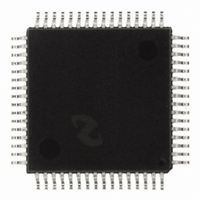
CLC018AJVJQ/NOPB National Semiconductor, CLC018AJVJQ/NOPB Datasheet - Page 9

CLC018AJVJQ/NOPB
Manufacturer Part Number
CLC018AJVJQ/NOPB
Description
IC CROSSPOINT SWITCH 8X8 64PQFP
Manufacturer
National Semiconductor
Datasheet
1.CLC018AJVJQNOPB.pdf
(17 pages)
Specifications of CLC018AJVJQ/NOPB
Function
Crosspoint Switch
Circuit
1 x 8:8
Voltage Supply Source
Dual Supply
Voltage - Supply, Single/dual (±)
±4.5 V ~ 5.5 V
Operating Temperature
-40°C ~ 85°C
Mounting Type
Surface Mount
Package / Case
64-QFP
Lead Free Status / RoHS Status
Lead free / RoHS Compliant
Other names
*CLC018AJVJQ
*CLC018AJVJQ/NOPB
CLC018AJVJQ
*CLC018AJVJQ/NOPB
CLC018AJVJQ
Available stocks
Company
Part Number
Manufacturer
Quantity
Price
Company:
Part Number:
CLC018AJVJQ/NOPB
Manufacturer:
IDT
Quantity:
300
Company:
Part Number:
CLC018AJVJQ/NOPB
Manufacturer:
Texas Instruments
Quantity:
10 000
Operation
POWER SUPPLIES, GROUNDING AND BYPASSING
The CLC018 uses separate power supplies for control and
data circuitry. Data circuitry is supplied via V
circuitry via V
supply, is the common return for both. Connection details for
the different powering modes is shown in Table 1.
Internal and external capacitances, normal and parasitic,
must be charged and discharged with changes in output
voltage. Charging current depends upon the size of these
capacitances and the rate of change of voltage. At the fast
transition times of the CLC016, small amounts of stray ca-
pacitance at outputs can produce large output and supply
transient currents. Controlling transient currents requires
particular attention to minimizing stray capacitances and to
providing effective bypassing in the design. Good and effec-
tive bypassing consisting of 0.01 µF to 0.1 µF monolithic
ceramic and 4.7 µF to 10 µF, 35V tantalum capacitors. These
capacitors should be placed as close to power pins as
practical and tightly connected to the power plane sandwich
using multiple vias. Needless to say, multilayer board tech-
nology should be employed for the CLC018 and similar
high-frequency-capability devices.
CONFIGURING THE SWITCH
The CLC018 can be configured so that any output may be
independently connected to any input and any input be
connected to any or all outputs. Each output may be inde-
pendently enabled or placed in a high-impedance state.
Data controlling the switch matrix and output mode are
stored in two ranks of eight, 4-bit registers, one register per
output. The three most-significant bits in each register iden-
tify the input to be connected to that output. The least-
FIGURE 10. 1.485 Gbps Eye Pattern
LL
. Supply connection V
(Continued)
EE
, the negative-most
CC
10008826
and control
9
significant bit controls whether the output is active or TRI-
STATE. A particular register in the first rank, the LOAD
REGISTERS, is selected by a 3-bit word placed on the
output address (OA) bus. Data to be written into the load
register, consisting of the 3-bit address of the input to be
connected to that output and the output-enable control bit,
are placed on the input address (IA) bus. Input data is stored
in the load registers at the low-to-high transition of the LOAD
input pin with chip-select (CS) high-true. The contents of the
load registers are transferred to the second rank of CON-
FIGURATION REGISTERS at the low-to-high transition of
the CNFG input signal (with CS high). This causes the state
of the entire switch matrix to be set to the selected configu-
ration.
The entire crosspoint may be placed in an initializing state,
with all outputs connected to input-0 and with all outputs
either enabled or TRI-STATE. To do so, hold TRI low to make
outputs active, or high to place outputs in TRI-STATE, and
apply a high-going pulse to the RES input pin (with CS high).
In summary, outputs are configured by:
a) first placing the 3-bit address of that output on the OA
b) the 3-bit address of the input to be connected to that
c) the output-enable (TRI-STATE) control bit for that output
d) making chip-select (CS) true, and then
e) providing a high-going pulse to the LOAD input pin.
f)
The entire crosspoint matrix may now be configured with the
data held in the load registers. To implement the configura-
tion, apply a high-going pulse to the CNFG input pin. The
contents of the load registers are transferred to the configu-
ration registers and the new configuration of all crosspoints
is effected.
The CLC018 Configuration Truth Table is shown at the end
of the datasheet.
EXPANDING THE SWITCH SIZE
The CLC018 was designed for easy expansion to larger
array sizes without paying a significant penalty in either
speed or power. The power dissipation of the expanded
array will be dominated by the number of active outputs,
therefore power will increase linearly with the array size even
though the number of components required increases as the
square of the array size. As an example, a single CLC018
can be used for an 8x8 array, and it will dissipate about
0.85W. A 32 x 32 array will require 16 CLC018s and will
consume only about 4W.
bus together with
output on the IA bus,
on the IA bus,
Repeat these four steps for each output to be
configured.
www.national.com


