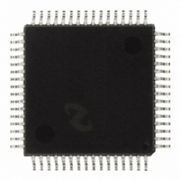
CLC018AJVJQ/NOPB National Semiconductor, CLC018AJVJQ/NOPB Datasheet - Page 5

CLC018AJVJQ/NOPB
Manufacturer Part Number
CLC018AJVJQ/NOPB
Description
IC CROSSPOINT SWITCH 8X8 64PQFP
Manufacturer
National Semiconductor
Datasheet
1.CLC018AJVJQNOPB.pdf
(17 pages)
Specifications of CLC018AJVJQ/NOPB
Function
Crosspoint Switch
Circuit
1 x 8:8
Voltage Supply Source
Dual Supply
Voltage - Supply, Single/dual (±)
±4.5 V ~ 5.5 V
Operating Temperature
-40°C ~ 85°C
Mounting Type
Surface Mount
Package / Case
64-QFP
Lead Free Status / RoHS Status
Lead free / RoHS Compliant
Other names
*CLC018AJVJQ
*CLC018AJVJQ/NOPB
CLC018AJVJQ
*CLC018AJVJQ/NOPB
CLC018AJVJQ
Available stocks
Company
Part Number
Manufacturer
Quantity
Price
Company:
Part Number:
CLC018AJVJQ/NOPB
Manufacturer:
IDT
Quantity:
300
Company:
Part Number:
CLC018AJVJQ/NOPB
Manufacturer:
Texas Instruments
Quantity:
10 000
Connection Diagram
Pin Descriptions
POWER PINS
V
levels are ECL compatible, then V
GND. For PECL data (+5V referenced ECL), V
nected to the +5V supply. Please refer to the device opera-
tion section in this datasheet for recommendations on the
bypassing and ground/power plane requirements of this de-
vice.
V
levels are ECL compatible, then V
power supply. For PECL data (+5V referenced ECL), V
connected to GND.
V
referenced to +5V, V
control signals are ECL compatible, V
GND.
DATA INPUT PINS
DI0 and DI0 through DI7 and D17 are the data input pins to
the CLC018. Depending upon how the Power pins are con-
nected (please refer to the Power Pin section above) the
data may be either differential ECL, or differential PECL. To
drive the CLC018 inputs with a single-ended signal, please
refer to the section “Using Single-Ended Data” in the OP-
ERATION section of this datasheet.
DATA OUTPUT PINS
DO0 and DO0 through DO7 and DO7 are the data output
pins of the CLC018. The CLC018 outputs are differential
current outputs which can be converted to ECL or PECL
compatible outputs through the use of load resistors. Please
refer to the “Output Interfacing” paragraph in the OPERA-
TION section of this datasheet for more details.
CONTROL PINS
IA2, IA1 and IA0 are the three bit input selection address
bus. The input port to be addressed is placed on this bus.
IA2 is the Most Significant Bit (MSB). If input port 6 is to be
CC
EE
LL
is the logic-level power supply. If the control signals are
is the most negative rail for the data path. When the data
is the most positive rail for the data path. When the data
LL
is connected to a +5V supply. If
CC
EE
is connected to a −5.2V
should be connected to
LL
is connected to
See NS Package Number VJQ64A
Order Number CLC018AJVJQ
CC
is con-
EE
is
5
addressed, IA2, IA1, IA0 should have 1, 1, 0 asserted on
them. The IA bus should be driven with CMOS levels, if V
is +5V. These levels are thus +5V referenced (standard
CMOS). If V
referenced to the −5V and GND supplies.
OA2, OA1 and OA0 are the output selection address bus.
The output port selected by the OA bus is connected to the
input port selected on the IA bus when the data is loaded into
the configuration registers. OA2 is the MSB. If OA2, OA1,
OA0 are set to 0, 0, 1; then output port 1 will be selected.
CS is an active-high chip select input. When CS is high, the
RES, LOAD, and CNFG pins will be enabled.
LOAD is the latch control for the LOAD register. When LOAD
is high, the load register is transparent. Outputs follow the
state of the IA bus, and are presented to the inputs of the
Configuration register selected by the OA bus. When LOAD
is low, the outputs of the Load register are latched.
RES is the reset control of the configuration and load regis-
ters. A high-going pulse on the RES pin programs the switch
matrix to one of two possible states: with TRI low, all outputs
are connected to input #0; with TRI high, all outputs are put
in TRI-STATE condition.
TRI will program the selected output to be in a high imped-
ance or TRI-STATE condition. To place an output in TRI-
STATE, assert a logic-high level on the TRI input when the
desired input and output addresses are asserted on the
respective address inputs and strobe the LOAD input as
depicted in the ”Configuration Truth Table”. To enable an
output, assert a logic-low level on the TRI input together with
the appropriate addresses and strobe the LOAD input as
previously described.
CNFG is the configuration register latch control. When
CNFG is high the Configuration register is made transparent,
and the switch matrix is set to the state loaded into the Load
registers. When CNFG is low, the state of the switch matrix
is latched.
LL
10008809
is connected to GND, the input levels are
www.national.com
LL


