MICRF620 Micrel Inc, MICRF620 Datasheet
MICRF620
Specifications of MICRF620


Related parts for MICRF620

MICRF620 Summary of contents
Page 1
... General Description The MICRF620 is a self-contained frequency shift keying (FSK) transceiver module, intended for use in half-duplex, bidirectional RF links. The transceiver module is intended for UHF radio equipment in compliance with the European Standard Institute (ETSI) specification, EN300 220. The transmitter consists of a fully programmable PLL frequency synthesizer and power amplifier ...
Page 2
... Programming........................................................................................................................................................................... 7 General ............................................................................................................................................................................... 7 Writing to the Control Registers in MICRF620 ................................................................................................................... 8 Writing to a Single Register ................................................................................................................................................ 8 Writing to All Registers ....................................................................................................................................................... 8 Writing to n Registers Having Incremental Addresses ....................................................................................................... 9 Reading from the Control Registers in MICRF620 ............................................................................................................. 9 Reading n Registers from MICRF620................................................................................................................................. 9 Programming Interface Timing.............................................................................................................................................. 10 Power on Reset ................................................................................................................................................................ 11 Programming Summary.................................................................................................................................................... 11 Frequency Synthesizer ......................................................................................................................................................... 12 Crystal Oscillator (XCO) ................................................................................................................................................... 12 VCO ...
Page 3
... Receive Voltage <20 kbps 13.5 mA 2.0-2.5 v Lead-free MICRF600 <15 kbps 13.5 mA 2.0-2.5 v Lead-free MICRF610 <20 kbps 12.0 mA 2.0-2.5 v Lead-free MICRF620 19.2 kbaud 8 mA 2.5-3.4 V 19.2 kbaud 10 mA 2.5-3.4 V 19.2 kbaud 10 mA 2.5-3.4 V (1) Junction Temp. Range –20° to +75°C –20° to +75°C ...
Page 4
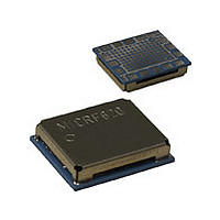
... GND 11 GND 12 GND 13 ANT 14 GND 15 VDD 16 GND July 2006 MICRF620 TR 11.5 x 14.1 mm (Top view) Type Pin Function Not connected Not connected I Chip select, three wire programming interface I Clock, three wire programming interface I/O Data, three wire programming interface I/O Data receive/transmit, bi-directional ...
Page 5
... PA2_0: 111 LOAD R = 50Ω, PA2_0: 001 LOAD R = 50Ω, PA2_0: 111 LOAD Limited by receiver BW NRZ 19.2kbps, β (±85kHz), -36dBm (RBW=10kHz) ETSI EN300 220 5 MICRF620/MICRF620Z (2) ) ..................................+2.0V to +2. .......................–20°C to +75°C A < +75°C, unless noted. A Min Typ Max 2.0 2.5 0.3 ...
Page 6
... Offset ±1MHz Desired signal: Offset ±2MHz 19.2 kbps, β =6, Offset ±5MHz 3dB above sens, Offset ±10MHz SC=133 kHz Offset ±30MHz 2 tones with 1MHz separation ETSI 300-220 Pin = -100 dBm Pin = -60 dBm 6 MICRF620/MICRF620Z Min Typ Max 12 10.3 9.6 3 -110 -109 -108 -107 -105 +10 ...
Page 7
... The MICRF620 will ignore transitions on the SCLK line if the CS line is inactive. The MICRF620 can be put on a bus, sharing clock and data lines with other devices. All control registers should be written to after a battery reset ...
Page 8
... Making these events is referred “write sequence.” possible to update all control registers in a write sequence. The address to write to (or the first address to write to) can be any valid address (0-21). The IO line is always an input to the MICRF620 (output from user) when writing. What to write: • ...
Page 9
... It is possible to read all registers. The address to read from (or the first address to read from) can be any valid address (0-22). Reading is not destructive, i.e. values are not changed. The IO line is output from the MICRF620 (input to user) for a part of the read-sequence. Refer to procedure description below. ...
Page 10
... Min. delay from rising edge of SCLK to valid IO during a read operation (assuming load capacitance 25pF) Table 6. Timing Specification for the 3-wire Programming Interface July 2006 traise Tper Thigh tfall Tlow Address Register Figure 4. Programming Interface Timing 10 MICRF620/MICRF620Z Tread Twrite Tscl Data Register LOAD Values Min. Typ ...
Page 11
... Micrel, Inc. Power on Reset When applying voltage to the MICRF620 a power on reset state is entered. During the time period of power on reset, the MICRF620 should be considered unknown state and the user should wait until completed (See Table 6). The power on reset timing given in table 6 is covering all conditions and should be treated as a maximum delay time ...
Page 12
... The bias bit will optimize the phase noise, and the frequency bit will control a capacitor bank in the VCO. The tuning range the RF frequency versus varactor voltage is dependent on the VCO frequency setting, and can be shown in Figure 6. When XCOtune4 – 12 MICRF620/MICRF620Z 55.0 45.0 35.0 25.0 15.0 5.0 -5 ...
Page 13
... Mode1 Mode0 State Comments 0 0 Power down Keeps register configuration 0 1 Standby Only crystal oscillator running 1 0 Receive Full receive 1 1 Transmit Full transmit ex PA state July 2006 1,6 2 2,4 = 2.5V LD_en PF_FC1 PF_FC0 Sync_en Mode1 Mode0 ’1’ 13 MICRF620/MICRF620Z M9999-120205 ...
Page 14
... DATACLK and DATAIXO in receive mode and transmit mode. MICRF620 will present data on rising edge and the “USER” sample data on falling edge in receive mode. DATAIXO Bit synchronizer. The DATACLK The User presents data on falling edge and MICRF620 samples on rising edge in transmit mode. f XCO (7 -BITRATE_c lkS) × 2 ...
Page 15
... A formula for the receiver bandwidth can be summarized as follows LD_en PF_FC1 PF_FC0 In battery operated applications that do not need very high selectivity, the main channel filter can be bypassed by SC_by=1. This will reduce the Rx current consumption with ~2mA. Cut-off Freq. (kHz) 15 MICRF620/MICRF620Z ‘ ...
Page 16
... To compensate for this, the receivers XCO frequency should be increased recommended to use Mode UP+DN for two reasons, you do not need to know the actual frequency deviation and this mode gives the best accuracy. 16 MICRF620/MICRF620Z FEEC_1 FEEC_0 FEE Mode 0 0 Off ...
Page 17
... A procedure for using the XCO tuning feature in combination with the FEE is given below. The MICRF620 measures the frequency offset between the receivers LO frequency and the frequency of the transmitter. The receiver XCO frequency can be tuned until the receiver and transmitter frequencies are equal ...
Page 18
... Figure 11 shows a recommended voltage divider circuit for a MCU running at 3.0V and the MICRF620 at 2.5V. July 2006 MICRF6xx CS SCLK IO DATAIXO DATACLK LD RSSI Figure 12. How to connect MICRF620 (2.5V) and MCU (3.0V) and a mikro- 18 MICRF620/MICRF620Z MCU 3k3 CS 18k 3k3 SCLK 18k 3k3 ...
Page 19
... Micrel, Inc. Assembling the MICRF620 Recommended Reflow Temperature Profile When the MICRF620 module is being automatically assembled to a PCB, care must be taken not to expose the module for temperature above the maximum specified. Figure 13 shows the recommended reflow temperature profile. Figure 13. Recommended Reflow Temperature Reflow ...
Page 20
... Digital high speed should/must safe distance from RF circuitry or RF VDD as this might/will cause degradation of sensitivity and create spurious emissions. Example of such circuitry is LCD display, charge pumps, RS232, clock / data bus etc. 20 MICRF620/MICRF620Z logic or noisy circuitry M9999-120205 ...
Page 21
... Purchaser’s use or sale of Micrel Products for use in life support appliances, devices or systems is a Purchaser’s own risk and Purchaser agrees to fully July 2006 Figure 15. Package Dimensions Figure 16. Tape Dimensions indemnify Micrel for any damages resulting from such use or sale. © 2005 Micrel, Incorporated. 21 MICRF620/MICRF620Z nt M9999-120205 ...