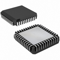
DS2153Q-A7+T&R Maxim Integrated Products, DS2153Q-A7+T&R Datasheet - Page 39

DS2153Q-A7+T&R
Manufacturer Part Number
DS2153Q-A7+T&R
Description
IC TXRX E1 1-CHIP 5V 44-PLCC
Manufacturer
Maxim Integrated Products
Datasheet
1.DS2153Q-A7TR.pdf
(60 pages)
Specifications of DS2153Q-A7+T&R
Function
Single-Chip Transceiver
Interface
E1
Number Of Circuits
1
Voltage - Supply
4.75 V ~ 5.25 V
Current - Supply
65mA
Operating Temperature
0°C ~ 70°C
Mounting Type
Surface Mount
Package / Case
*
Lead Free Status / RoHS Status
Lead free / RoHS Compliant
Power (watts)
-
13 LINE INTERFACE FUNCTIONS
The line interface function in the DS2153Q contains three sections: the receiver, which handles clock and
data recovery; the transmitter, which waveshapes and drives the T1 line; and the jitter attenuator. Each of
these three sections is controlled by the Line Interface Control Register (LICR), which is described
below.
LICR: LINE INTERFACE CONTROL REGISTER (Address = 18 Hex)
(MSB)
LB2
LB1
SYMBOL POSITION NAME AND DESCRIPTION
JABDS
EGL
TPD
DJA
LB2
LB1
LB0
JAS
LB0
LICR.7
LICR.6
LICR.5
LICR.4
LICR.3
LICR.2
LICR.1
LICR.0
EGL
Line Build-Out Select Bit 2. Sets the transmitter build
out; see the
Line Build-Out Select Bit 1. Sets the transmitter build
out; see the
Line Build-Out Select Bit 0. Sets the transmitter build
out; see the
Receive Equalizer Gain Limit.
0 = -12dB
1 = -30dB
Jitter Attenuator Select.
0 = place the jitter attenuator on the receive side
1 = place the jitter attenuator on the transmit side
Jitter Attenuator Buffer Depth Select.
0 = 128 bits
1 = 32 bits (use for delay sensitive applications)
Disable Jitter Attenuator.
0 = jitter attenuator enabled
1 = jitter attenuator disabled
Transmit Power Down.
0 = normal transmitter operation
1 = powers down the transmitter and tri-states the TTIP
and TRING pins
39 of 60
JAS
Table
Table
Table
JABDS
13-2.
13-2.
13-2.
DJA
(LSB)
TPD
LICR


