DS3170+ Maxim Integrated Products, DS3170+ Datasheet - Page 33
DS3170+
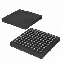
Manufacturer Part Number
DS3170+
Description
IC TXRX DS3/E3 100-CSBGA
Manufacturer
Maxim Integrated Products
Datasheet
1.DS3170.pdf
(230 pages)
Specifications of DS3170+
Function
Single-Chip Transceiver
Interface
DS3, E3
Number Of Circuits
1
Voltage - Supply
3.135 V ~ 3.465 V
Current - Supply
120mA
Operating Temperature
0°C ~ 70°C
Mounting Type
Surface Mount
Package / Case
100-LBGA
Includes
DS3 Framers, E3 Framers, HDLC Controller, On-Chip BERTs
Lead Free Status / RoHS Status
Lead free / RoHS Compliant
Power (watts)
-


D[15:8]
D[7]/
SPI_CPOL
D[6]/
SPI_CPHA
D[5]/
SPI_SWAP
D[4:3]
D[2]/
SPI_SCLK
D[1]/
SPI_MOSI
D[0]/
SPI_MISO
A[8:1]
A[0] /
BSWAP
ALE
PIN NAME
TYPE
IO
IO
IO
IO
IO
IO
IO
IO
I
I
positions of the data on the RSER pin. The signal goes high during each DS3/E3
payload bit and goes low during each DS3/E3 overhead bit. The signal is updated on
the positive clock edge of the referenced clock pin if the clock pin signal is not
inverted, otherwise it is updated on the falling edge of the clock. The signal is typically
referenced to the RCLKO receive clock output pin, but it can be referenced to the
RLCLK clock input pin.
This signal can be inverted.
Upper 8 Bits of the Bi-directional 16 or 8 bit data bus
D[15:8]: Upper bits of the 16-bit or 8-bit data bus used to input data during register
writes, and data outputs during register reads. The upper 8 bits are not used in 8 bit
bus mode. Not driven when CS=1 or RST=0.
Bit 7 of Bi-directional data bus / SPI Bus Clock Polarity
D[7]: Bit 7 of the 16-bit or 8-bit data bus used to input data during register writes, and
data outputs during register reads. Not driven when CS=1 or RST=0.
SPI_CPOL: This signal selects the clock polarity when SPI = 1. See Section
for detailed timing and functionality information. Default setting is low.
Bit 6 of Bi-directional data bus / SPI Bus Clock Phase
D[6]: Bit 6 of the 16-bit or 8-bit data bus used to input data during register writes, and
data outputs during register reads. Not driven when CS=1 or RST=0.
SPI_CPHA: This signal selects the clock phase when SPI = 1. See Section
detailed timing and functionality information. Default setting is low.
Bit 5 of Bi-directional data bus / SPI Bit Order Swap
D[5]: Bit 5 of the 16-bit or 8-bit data bus used to input data during register writes, and
data outputs during register reads. Not driven when CS=1 or RST=0.
SPI_SWAP: This signal is active when SPI=1. The address and data bit order is
swapped when SPI_SWAP is high. The R/W and B bit positions are never changed in
the control word.
0 = MSB is transmitted and received first.
1 = LSB is transmitted and received first.
Bits 4,3 of Bi-directional data bus
D[4:3]: Bits 3,4 of the 16-bit or 8-bit data bus used to input data during register writes,
and data outputs during register reads. Not driven when CS=1 or RST=0.
Bit 2 of Bi-directional data bus / SPI Serial Clock Input < 10 MHz
D[2]: Bit 2 of the 16-bit or 8-bit data bus used to input data during register writes, and
data outputs during register reads. Not driven when CS=1 or RST=0.
SPI_SCLK: SPI Serial Clock Input when SPI = 1.
Bit 1 of Bi-directional data bus / SPI Serial Bus Master-out Slave-in
D[1]: Bit 1 of the 16-bit or 8-bit data bus used to input data during register writes, and
data outputs during register reads. Not driven when CS=1 or RST=0.
SPI_MOSI: SPI Serial Data Input (Master-out Slave-in) when SPI = 1.
Bit 0 of Bi-directional data bus / SPI Serial Bus Master-in Slave-out
D[0]: Bit 0 of the 16-bit or 8-bit data bus used to input data during register writes, and
data outputs during register reads. Not driven when CS=1 or RST=0.
SPI_MISO: SPI Serial Data Output (Master-in Slave-Out) when SPI = 1.
Address bus (minus LSB) / Device Address [8:1]
A[8:1]: identifies the specific 16 bit registers, or group of 8 bit registers, being
accessed.
Address bus LSB / Byte Swap / Device Address [0]
A[0]: This signal is connected to the lower address bit in 8 bit systems. (WIDTH=0)
BSWAP: This signal is tied high or low in 16 bit systems. (WIDTH=1)
Address Latch Enable
ALE: This signal is used to latch the address on the A[10:0] pins in multiplexed
1 = Output register bits 15:8 on D[7:0], D[15:8] not driven
0 = Output register bits 7:0 on D[7:0], D[15:8] not driven
1 = Output register bits 15:8 on D[7:0], 7:0 on D[15:8]
0 = Output register bits 7:0 on D[7:0], 15:8 on D[15:8]
Microprocessor Interface
33 of 230
PIN DESCRIPTION
DS3170 DS3/E3 Single-Chip Transceiver
8.3.4.1
8.3.4.1
for
Related parts for DS3170+
Image
Part Number
Description
Manufacturer
Datasheet
Request
R

Part Number:
Description:
MAX7528KCWPMaxim Integrated Products [CMOS Dual 8-Bit Buffered Multiplying DACs]
Manufacturer:
Maxim Integrated Products
Datasheet:
Part Number:
Description:
Single +5V, fully integrated, 1.25Gbps laser diode driver.
Manufacturer:
Maxim Integrated Products
Datasheet:
Part Number:
Description:
Single +5V, fully integrated, 155Mbps laser diode driver.
Manufacturer:
Maxim Integrated Products
Datasheet:
Part Number:
Description:
VRD11/VRD10, K8 Rev F 2/3/4-Phase PWM Controllers with Integrated Dual MOSFET Drivers
Manufacturer:
Maxim Integrated Products
Datasheet:
Part Number:
Description:
Highly Integrated Level 2 SMBus Battery Chargers
Manufacturer:
Maxim Integrated Products
Datasheet:
Part Number:
Description:
Current Monitor and Accumulator with Integrated Sense Resistor; ; Temperature Range: -40°C to +85°C
Manufacturer:
Maxim Integrated Products
Part Number:
Description:
TSSOP 14/A�/RS-485 Transceivers with Integrated 100O/120O Termination Resis
Manufacturer:
Maxim Integrated Products
Part Number:
Description:
TSSOP 14/A�/RS-485 Transceivers with Integrated 100O/120O Termination Resis
Manufacturer:
Maxim Integrated Products
Part Number:
Description:
QFN 16/A�/AC-DC and DC-DC Peak-Current-Mode Converters with Integrated Step
Manufacturer:
Maxim Integrated Products
Part Number:
Description:
TDFN/A/65V, 1A, 600KHZ, SYNCHRONOUS STEP-DOWN REGULATOR WITH INTEGRATED SWI
Manufacturer:
Maxim Integrated Products
Part Number:
Description:
Integrated Temperature Controller f
Manufacturer:
Maxim Integrated Products
Part Number:
Description:
SOT23-6/I�/45MHz to 650MHz, Integrated IF VCOs with Differential Output
Manufacturer:
Maxim Integrated Products
Part Number:
Description:
SOT23-6/I�/45MHz to 650MHz, Integrated IF VCOs with Differential Output
Manufacturer:
Maxim Integrated Products
Part Number:
Description:
EVALUATION KIT/2.4GHZ TO 2.5GHZ 802.11G/B RF TRANSCEIVER WITH INTEGRATED PA
Manufacturer:
Maxim Integrated Products
Part Number:
Description:
QFN/E/DUAL PCIE/SATA HIGH SPEED SWITCH WITH INTEGRATED BIAS RESISTOR
Manufacturer:
Maxim Integrated Products
Datasheet: