SC16IS740IPW,112 NXP Semiconductors, SC16IS740IPW,112 Datasheet - Page 8
SC16IS740IPW,112
Manufacturer Part Number
SC16IS740IPW,112
Description
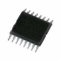
IC UART SINGLE W/FIFO 16-TSSOP
Manufacturer
NXP Semiconductors
Type
UART with 64-byte FIFOs and IrDA encoder/decoderr
Datasheet
1.SC16IS740IPW112.pdf
(62 pages)
Specifications of SC16IS740IPW,112
Number Of Channels
1, UART
Package / Case
16-TSSOP (0.173", 4.40mm Width)
Fifo's
64 Byte
Protocol
RS232, RS485
Voltage - Supply
2.5V, 3.3V, 5V
With Auto Flow Control
Yes
With False Start Bit Detection
Yes
With Modem Control
Yes
Mounting Type
Surface Mount
Data Rate
5 Mbps
Supply Voltage (max)
3.6 V
Supply Voltage (min)
2.3 V
Supply Current
6 mA
Maximum Operating Temperature
+ 85 C
Minimum Operating Temperature
- 40 C
Mounting Style
SMD/SMT
Operating Supply Voltage
2.5 V, 3.3 V
Lead Free Status / RoHS Status
Lead free / RoHS Compliant
For Use With
568-4000 - DEMO BOARD SPI/I2C TO DUAL UART568-3510 - DEMO BOARD SPI/I2C TO UART
Lead Free Status / Rohs Status
Lead free / RoHS Compliant
Other names
568-3648-5
935280988112
SC16IS740IPW
935280988112
SC16IS740IPW
Available stocks
Company
Part Number
Manufacturer
Quantity
Price
Company:

Part Number:
SC16IS740IPW,112
Manufacturer:
JAMICON
Quantity:
101


NXP Semiconductors
Table 2.
[1]
[2]
SC16IS740_750_760_6
Product data sheet
Symbol
CS/A0
SI/A1
SO
SCL/SCLK
SDA
IRQ
GPIO0
GPIO1
GPIO2
GPIO3
GPIO4/DSR -
GPIO5/DTR -
GPIO6/CD
GPIO7/RI
RTS
V
V
SS
SS
See
Selectable with IOControl register bit 1.
Section 7.4 “Hardware reset, Power-On Reset (POR) and software reset”
Pin description
Pin
TSSOP16 TSSOP24 HVQFN24
2
3
4
5
6
7
-
-
-
-
-
-
10
9
-
9
10
11
12
13
14
15
16
17
18
20
21
22
23
24
19
-
…continued
6
7
8
9
10
11
12
13
14
15
17
18
19
20
21
16
center
pad
[3]
[3]
Single UART with I
Rev. 06 — 13 May 2008
Type Description
I
I
O
I
I/O
O
I/O
I/O
I/O
I/O
I/O
I/O
I/O
I/O
O
-
-
SPI chip select or I
configuration is selected by I2C/SPI pin, this pin is the SPI chip
select pin (Schmitt-trigger, active LOW). If I
is selected by I2C/SPI pin, this pin along with A1 pin allows user
to change the device’s base address.
SPI data input pin or I
configuration is selected by I2C/SPI pin, this is the SPI data
input pin. If I
pin along with A0 pin allows user to change the device’s base
address. To select the device address, please refer to
SPI data output pin. If SPI configuration is selected by I2C/SPI
pin, this is a 3-stateable output pin. If I
selected by I2C/SPI pin, this pin function is undefined and must
be left as n.c. (not connected).
I
I
selected by I2C/SPI pin. If SPI configuration is selected then this
pin is an undefined pin and must be connected to V
Interrupt (open-drain, active LOW). Interrupt is enabled when
interrupt sources are enabled in the Interrupt Enable Register
(IER). Interrupt conditions include: change of state of the input
pins, receiver errors, available receiver buffer data, available
transmit buffer space, or when a modem status flag is detected.
An external resistor (1 k for 3.3 V, 1.5 k for 2.5 V) must be
connected between this pin and V
programmable I/O pin
programmable I/O pin
programmable I/O pin
programmable I/O pin
programmable I/O pin or modem’s DSR pin
programmable I/O pin or modem’s DTR pin
programmable I/O pin or modem’s CD pin
programmable I/O pin or modem’s RI pin
UART request to send (active LOW). A logic 0 on the RTS pin
indicates the transmitter has data ready and waiting to send.
Writing a logic 1 in the modem control register MCR[1] will set
this pin to a logic 0, indicating data is available. After a reset this
pin is set to a logic 1. This pin only affects the transmit and
receive operations when auto RTS function is enabled via the
Enhanced Feature Register (EFR[6]) for hardware flow control
operation.
ground
The center pad on the back side of the HVQFN24 package is
metallic and should be connected to ground on the
printed-circuit board.
2
2
C-bus or SPI input clock.
C-bus data input/output, open-drain if I
2
2
C-bus/SPI interface, 64-byte FIFOs, IrDA SIR
C-bus configuration is selected by I2C/SPI pin, this
2
SC16IS740/750/760
C-bus device address select A0. If SPI
2
C-bus device address select A1. If SPI
DD
.
2
C-bus configuration is
2
[2]
C-bus configuration is
[2]
2
[2]
[2]
C-bus configuration
© NXP B.V. 2008. All rights reserved.
SS
.
Table
8 of 62
32.
Related parts for SC16IS740IPW,112
Image
Part Number
Description
Manufacturer
Datasheet
Request
R

Part Number:
Description:
NXP Semiconductors designed the LPC2420/2460 microcontroller around a 16-bit/32-bitARM7TDMI-S CPU core with real-time debug interfaces that include both JTAG andembedded trace
Manufacturer:
NXP Semiconductors
Datasheet:

Part Number:
Description:
NXP Semiconductors designed the LPC2458 microcontroller around a 16-bit/32-bitARM7TDMI-S CPU core with real-time debug interfaces that include both JTAG andembedded trace
Manufacturer:
NXP Semiconductors
Datasheet:
Part Number:
Description:
NXP Semiconductors designed the LPC2468 microcontroller around a 16-bit/32-bitARM7TDMI-S CPU core with real-time debug interfaces that include both JTAG andembedded trace
Manufacturer:
NXP Semiconductors
Datasheet:
Part Number:
Description:
NXP Semiconductors designed the LPC2470 microcontroller, powered by theARM7TDMI-S core, to be a highly integrated microcontroller for a wide range ofapplications that require advanced communications and high quality graphic displays
Manufacturer:
NXP Semiconductors
Datasheet:
Part Number:
Description:
NXP Semiconductors designed the LPC2478 microcontroller, powered by theARM7TDMI-S core, to be a highly integrated microcontroller for a wide range ofapplications that require advanced communications and high quality graphic displays
Manufacturer:
NXP Semiconductors
Datasheet:
Part Number:
Description:
The Philips Semiconductors XA (eXtended Architecture) family of 16-bit single-chip microcontrollers is powerful enough to easily handle the requirements of high performance embedded applications, yet inexpensive enough to compete in the market for hi
Manufacturer:
NXP Semiconductors
Datasheet:
Part Number:
Description:
The XA-S3 device is a member of Philips Semiconductors? XA(eXtended Architecture) family of high performance 16-bitsingle-chip microcontrollers
Manufacturer:
NXP Semiconductors
Datasheet:

Part Number:
Description:
The NXP BlueStreak LH75401/LH75411 family consists of two low-cost 16/32-bit System-on-Chip (SoC) devices
Manufacturer:
NXP Semiconductors
Datasheet:
Part Number:
Description:
The NXP LPC3130/3131 combine an 180 MHz ARM926EJ-S CPU core, high-speed USB2
Manufacturer:
NXP Semiconductors
Datasheet:
Part Number:
Description:
The NXP LPC3141 combine a 270 MHz ARM926EJ-S CPU core, High-speed USB 2
Manufacturer:
NXP Semiconductors
Part Number:
Description:
The NXP LPC3143 combine a 270 MHz ARM926EJ-S CPU core, High-speed USB 2
Manufacturer:
NXP Semiconductors

Part Number:
Description:
The NXP LPC3152 combines an 180 MHz ARM926EJ-S CPU core, High-speed USB 2
Manufacturer:
NXP Semiconductors
Part Number:
Description:
The NXP LPC3154 combines an 180 MHz ARM926EJ-S CPU core, High-speed USB 2
Manufacturer:
NXP Semiconductors

Part Number:
Description:
Standard level N-channel enhancement mode Field-Effect Transistor (FET) in a plastic package using NXP High-Performance Automotive (HPA) TrenchMOS technology
Manufacturer:
NXP Semiconductors
Datasheet: