SC16IS762IBS,151 NXP Semiconductors, SC16IS762IBS,151 Datasheet - Page 45
SC16IS762IBS,151
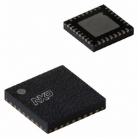
Manufacturer Part Number
SC16IS762IBS,151
Description
IC UART DUAL I2C/SPI 32-HVQFN
Manufacturer
NXP Semiconductors
Type
IrDA or RS- 232 or RS- 485r
Datasheet
1.SC16IS752IBS151.pdf
(59 pages)
Specifications of SC16IS762IBS,151
Number Of Channels
2, DUART
Package / Case
32-VFQFN Exposed Pad
Features
Low Current
Fifo's
64 Byte
Protocol
RS232, RS485
Voltage - Supply
2.5V, 3.3V
With Auto Flow Control
Yes
With False Start Bit Detection
Yes
With Modem Control
Yes
Mounting Type
Surface Mount
Data Rate
5 Mbps
Supply Voltage (max)
3.6 V
Supply Voltage (min)
2.3 V
Supply Current
6 mA
Maximum Operating Temperature
+ 95 C
Minimum Operating Temperature
- 40 C
Mounting Style
SMD/SMT
Operating Supply Voltage
2.5 V or 3.3 V
Lead Free Status / RoHS Status
Lead free / RoHS Compliant
For Use With
568-4000 - DEMO BOARD SPI/I2C TO DUAL UART568-3510 - DEMO BOARD SPI/I2C TO UART
Lead Free Status / Rohs Status
Lead free / RoHS Compliant
Other names
568-2240
935279293151
SC16IS762IBS-S
935279293151
SC16IS762IBS-S


NXP Semiconductors
14. Dynamic characteristics
Table 37.
All the timing limits are valid within the operating supply voltage, ambient temperature range and output load;
V
voltage of V
[1]
[2]
[3]
SC16IS752_SC16IS762_7
Product data sheet
Symbol
f
t
t
t
t
t
t
t
t
t
t
t
t
t
t
t
t
t
t
t
t
t
t
t
SCL
BUF
HD;STA
SU;STA
SU;STO
HD;DAT
VD;ACK
VD;DAT
SU;DAT
LOW
HIGH
f
r
SP
d1
d2
d3
d4
d5
d6
d7
d8
d15
w(rst)
DD
= 2.5 V
A detailed description of the I
manual” . This may be found at www.nxp.com/acrobat_download/usermanuals/UM10204_3.pdf.
Minimum SCL clock frequency is limited by the bus time-out feature, which resets the serial bus interface if SDA is held LOW for a
minimum of 25 ms.
2 XTAL1 clock cycles or 3 s, whichever is less.
SS
I
2
C-bus timing specifications
0.2 V, T
Parameter
SCL clock frequency
bus free time between a STOP and START
condition
hold time (repeated) START condition
set-up time for a repeated START condition
set-up time for STOP condition
data hold time
data valid acknowledge time
data valid time
data set-up time
LOW period of the SCL clock
HIGH period of the SCL clock
fall time of both SDA and SCL signals
rise time of both SDA and SCL signals
pulse width of spikes that must be
suppressed by the input filter
I
I
I
I2C input pin interrupt valid time
I2C input pin interrupt clear time
I
I
I
SCL delay after reset
reset pulse width
to V
2
2
2
2
2
2
C-bus GPIO output valid time
C-bus modem input interrupt valid time
C-bus modem input interrupt clear time
C-bus receive interrupt valid time
C-bus receive interrupt clear time
C-bus transmit interrupt clear time
DD
. All output load = 25 pF, except SDA output load = 400 pF.
amb
= 40 C to +85 C; or V
2
C-bus specification, with applications, is given in user manual UM10204: “I
[1]
DD
Dual UART with I
Rev. 07 — 19 May 2008
= 3.3 V
Conditions
SCL LOW to
data out valid
0.3 V, T
amb
2
SC16IS752/SC16IS762
C-bus/SPI interface, 64-byte FIFOs, IrDA SIR
= 40 C to +95 C; V
[2]
[3]
Standard-mode
Min
250
4.7
4.0
4.7
4.7
4.7
4.0
0.5
0.2
0.2
0.2
0.2
0.2
0.2
1.0
0
0
3
3
-
-
-
-
-
I
2
C-bus
1000
Max
100
300
0.6
0.6
50
-
-
-
-
-
-
-
-
-
-
-
-
-
-
-
-
-
-
IL
2
C-bus specification and user
and V
Min
150
1.3
0.6
0.6
0.6
1.3
0.6
0.5
0.2
0.2
0.2
0.2
0.2
0.2
0.5
Fast-mode
0
0
3
3
-
-
-
-
-
© NXP B.V. 2008. All rights reserved.
I
IH
2
C-bus
refer to input
Max
400
300
300
0.6
0.6
50
-
-
-
-
-
-
-
-
-
-
-
-
-
-
-
-
-
-
45 of 59
Unit
kHz
ns
ns
ns
ns
ns
ns
s
s
s
s
s
s
s
s
s
s
s
s
s
s
s
s
s
Related parts for SC16IS762IBS,151
Image
Part Number
Description
Manufacturer
Datasheet
Request
R

Part Number:
Description:
NXP Semiconductors designed the LPC2420/2460 microcontroller around a 16-bit/32-bitARM7TDMI-S CPU core with real-time debug interfaces that include both JTAG andembedded trace
Manufacturer:
NXP Semiconductors
Datasheet:

Part Number:
Description:
NXP Semiconductors designed the LPC2458 microcontroller around a 16-bit/32-bitARM7TDMI-S CPU core with real-time debug interfaces that include both JTAG andembedded trace
Manufacturer:
NXP Semiconductors
Datasheet:
Part Number:
Description:
NXP Semiconductors designed the LPC2468 microcontroller around a 16-bit/32-bitARM7TDMI-S CPU core with real-time debug interfaces that include both JTAG andembedded trace
Manufacturer:
NXP Semiconductors
Datasheet:
Part Number:
Description:
NXP Semiconductors designed the LPC2470 microcontroller, powered by theARM7TDMI-S core, to be a highly integrated microcontroller for a wide range ofapplications that require advanced communications and high quality graphic displays
Manufacturer:
NXP Semiconductors
Datasheet:
Part Number:
Description:
NXP Semiconductors designed the LPC2478 microcontroller, powered by theARM7TDMI-S core, to be a highly integrated microcontroller for a wide range ofapplications that require advanced communications and high quality graphic displays
Manufacturer:
NXP Semiconductors
Datasheet:
Part Number:
Description:
The Philips Semiconductors XA (eXtended Architecture) family of 16-bit single-chip microcontrollers is powerful enough to easily handle the requirements of high performance embedded applications, yet inexpensive enough to compete in the market for hi
Manufacturer:
NXP Semiconductors
Datasheet:
Part Number:
Description:
The XA-S3 device is a member of Philips Semiconductors? XA(eXtended Architecture) family of high performance 16-bitsingle-chip microcontrollers
Manufacturer:
NXP Semiconductors
Datasheet:

Part Number:
Description:
The NXP BlueStreak LH75401/LH75411 family consists of two low-cost 16/32-bit System-on-Chip (SoC) devices
Manufacturer:
NXP Semiconductors
Datasheet:
Part Number:
Description:
The NXP LPC3130/3131 combine an 180 MHz ARM926EJ-S CPU core, high-speed USB2
Manufacturer:
NXP Semiconductors
Datasheet:
Part Number:
Description:
The NXP LPC3141 combine a 270 MHz ARM926EJ-S CPU core, High-speed USB 2
Manufacturer:
NXP Semiconductors
Part Number:
Description:
The NXP LPC3143 combine a 270 MHz ARM926EJ-S CPU core, High-speed USB 2
Manufacturer:
NXP Semiconductors

Part Number:
Description:
The NXP LPC3152 combines an 180 MHz ARM926EJ-S CPU core, High-speed USB 2
Manufacturer:
NXP Semiconductors
Part Number:
Description:
The NXP LPC3154 combines an 180 MHz ARM926EJ-S CPU core, High-speed USB 2
Manufacturer:
NXP Semiconductors

Part Number:
Description:
Standard level N-channel enhancement mode Field-Effect Transistor (FET) in a plastic package using NXP High-Performance Automotive (HPA) TrenchMOS technology
Manufacturer:
NXP Semiconductors
Datasheet: