SC16C752BIBS,128 NXP Semiconductors, SC16C752BIBS,128 Datasheet - Page 22
SC16C752BIBS,128
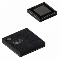
Manufacturer Part Number
SC16C752BIBS,128
Description
IC DUAL UART 64BYTE 32HVQFN
Manufacturer
NXP Semiconductors
Datasheet
1.SC16C752BIBS128.pdf
(47 pages)
Specifications of SC16C752BIBS,128
Features
False-start Bit Detection
Number Of Channels
2, DUART
Fifo's
64 Byte
Voltage - Supply
2.5V, 3.3V, 5V
With Auto Flow Control
Yes
With False Start Bit Detection
Yes
With Modem Control
Yes
Mounting Type
Surface Mount
Package / Case
32-VFQFN Exposed Pad
Lead Free Status / RoHS Status
Lead free / RoHS Compliant
Other names
935276389128
SC16C752BIBS-F
SC16C752BIBS-F
SC16C752BIBS-F
SC16C752BIBS-F


NXP Semiconductors
SC16C752B
Product data sheet
7.3 FIFO Control Register (FCR)
This is a write-only register that is used for enabling the FIFOs, clearing the FIFOs, setting
transmitter and receiver trigger levels, and selecting the type of DMA signalling.
shows FIFO control register bit settings.
Table 11.
Bit
7:6
5:4
3
2
1
0
Symbol
FCR[7] (MSB),
FCR[6] (LSB)
FCR[5] (MSB),
FCR[4] (LSB)
FCR[3]
FCR[2]
FCR[1]
FCR[0]
FIFO Control Register bits description
All information provided in this document is subject to legal disclaimers.
5 V, 2.2 V and 2.5 V dual UART, 5 Mbit/s (max.), with 64-byte FIFOs
DMA mode select.
Rev. 6 — 30 November 2010
Description
RX trigger. Sets the trigger level for the receive FIFO.
TX trigger. Sets the trigger level for the transmit FIFO.
FCR[5:4] can only be modified and enabled when EFR[4] is set. This is
because the transmit trigger level is regarded as an enhanced function.
Reset transmit FIFO.
Reset receive FIFO.
FIFO enable.
00 - 8 characters
01 - 16 characters
10 - 56 characters
11 - 60 characters
00 - 8 spaces
01 - 16 spaces
10 - 32 spaces
11 - 56 spaces
logic 0 = set DMA mode ‘0’
logic 1 = set DMA mode ‘1’
logic 0 = no FIFO transmit reset (normal default condition)
logic 1 = Clears the contents of the transmit FIFO and resets the FIFO
counter logic (the transmit shift register is not cleared or altered). This bit
will return to a logic 0 after clearing the FIFO.
logic 0 = no FIFO receive reset (normal default condition)
logic 1 = Clears the contents of the receive FIFO and resets the FIFO
counter logic (the receive shift register is not cleared or altered). This bit
will return to a logic 0 after clearing the FIFO.
logic 0 = disable the transmit and receive FIFO (normal default
condition)
logic 1 = enable the transmit and receive FIFO.
SC16C752B
© NXP B.V. 2010. All rights reserved.
Table 11
22 of 47
Related parts for SC16C752BIBS,128
Image
Part Number
Description
Manufacturer
Datasheet
Request
R

Part Number:
Description:
NXP Semiconductors designed the LPC2420/2460 microcontroller around a 16-bit/32-bitARM7TDMI-S CPU core with real-time debug interfaces that include both JTAG andembedded trace
Manufacturer:
NXP Semiconductors
Datasheet:

Part Number:
Description:
NXP Semiconductors designed the LPC2458 microcontroller around a 16-bit/32-bitARM7TDMI-S CPU core with real-time debug interfaces that include both JTAG andembedded trace
Manufacturer:
NXP Semiconductors
Datasheet:
Part Number:
Description:
NXP Semiconductors designed the LPC2468 microcontroller around a 16-bit/32-bitARM7TDMI-S CPU core with real-time debug interfaces that include both JTAG andembedded trace
Manufacturer:
NXP Semiconductors
Datasheet:
Part Number:
Description:
NXP Semiconductors designed the LPC2470 microcontroller, powered by theARM7TDMI-S core, to be a highly integrated microcontroller for a wide range ofapplications that require advanced communications and high quality graphic displays
Manufacturer:
NXP Semiconductors
Datasheet:
Part Number:
Description:
NXP Semiconductors designed the LPC2478 microcontroller, powered by theARM7TDMI-S core, to be a highly integrated microcontroller for a wide range ofapplications that require advanced communications and high quality graphic displays
Manufacturer:
NXP Semiconductors
Datasheet:
Part Number:
Description:
The Philips Semiconductors XA (eXtended Architecture) family of 16-bit single-chip microcontrollers is powerful enough to easily handle the requirements of high performance embedded applications, yet inexpensive enough to compete in the market for hi
Manufacturer:
NXP Semiconductors
Datasheet:
Part Number:
Description:
The XA-S3 device is a member of Philips Semiconductors? XA(eXtended Architecture) family of high performance 16-bitsingle-chip microcontrollers
Manufacturer:
NXP Semiconductors
Datasheet:

Part Number:
Description:
The NXP BlueStreak LH75401/LH75411 family consists of two low-cost 16/32-bit System-on-Chip (SoC) devices
Manufacturer:
NXP Semiconductors
Datasheet:
Part Number:
Description:
The NXP LPC3130/3131 combine an 180 MHz ARM926EJ-S CPU core, high-speed USB2
Manufacturer:
NXP Semiconductors
Datasheet:
Part Number:
Description:
The NXP LPC3141 combine a 270 MHz ARM926EJ-S CPU core, High-speed USB 2
Manufacturer:
NXP Semiconductors
Part Number:
Description:
The NXP LPC3143 combine a 270 MHz ARM926EJ-S CPU core, High-speed USB 2
Manufacturer:
NXP Semiconductors

Part Number:
Description:
The NXP LPC3152 combines an 180 MHz ARM926EJ-S CPU core, High-speed USB 2
Manufacturer:
NXP Semiconductors
Part Number:
Description:
The NXP LPC3154 combines an 180 MHz ARM926EJ-S CPU core, High-speed USB 2
Manufacturer:
NXP Semiconductors

Part Number:
Description:
Standard level N-channel enhancement mode Field-Effect Transistor (FET) in a plastic package using NXP High-Performance Automotive (HPA) TrenchMOS technology
Manufacturer:
NXP Semiconductors
Datasheet: