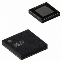
SC16C752BIBS,151 NXP Semiconductors, SC16C752BIBS,151 Datasheet - Page 30

SC16C752BIBS,151
Manufacturer Part Number
SC16C752BIBS,151
Description
IC UART DUAL W/FIFO 32-HVQFN
Manufacturer
NXP Semiconductors
Type
Dual UART with 64-byte FIFOsr
Datasheet
1.SC16C752BIBS151.pdf
(47 pages)
Specifications of SC16C752BIBS,151
Number Of Channels
2, DUART
Package / Case
32-VFQFN Exposed Pad
Features
False-start Bit Detection
Fifo's
64 Byte
Voltage - Supply
2.5V, 3.3V, 5V
With Auto Flow Control
Yes
With False Start Bit Detection
Yes
With Modem Control
Yes
Mounting Type
Surface Mount
Data Rate
5 Mbps
Supply Voltage (max)
5.5 V
Supply Voltage (min)
2.25 V
Supply Current
4.5 mA
Maximum Operating Temperature
+ 85 C
Minimum Operating Temperature
- 40 C
Mounting Style
SMD/SMT
Operating Supply Voltage
2.5 V or 3.3 V or 5 V
Lead Free Status / RoHS Status
Lead free / RoHS Compliant
Lead Free Status / RoHS Status
Lead free / RoHS Compliant, Lead free / RoHS Compliant
Other names
568-3288
935276389151
SC16C752BIBS-S
935276389151
SC16C752BIBS-S
NXP Semiconductors
SC16C752B
Product data sheet
7.13 Trigger Level Register (TLR)
7.14 FIFO ready register
This 8-bit register is pulsed to store the transmit and received FIFO trigger levels used for
DMA and interrupt generation. Trigger levels from 4 to 60 can be programmed with a
granularity of 4.
Table 21.
Remark: TLR can only be written to when EFR[4] = logic 1 and MCR[6] = logic 1. If
TLR[3:0] or TLR[7:4] are logic 0, the selectable trigger levels via the FIFO Control
Register (FCR) are used for the transmit and receive FIFO trigger levels. Trigger levels
from 4 bytes to 60 bytes are available with a granularity of four. The TLR should be
programmed for
When the trigger level setting in TLR is zero, the SC16C752B uses the trigger level setting
defined in FCR. If TLR has non-zero trigger level value, the trigger level defined in FCR is
discarded. This applies to both transmit FIFO and receive FIFO trigger level setting.
When TLR is used for RX trigger level control, FCR[7:6] should be left at the default state,
i.e., ‘00’.
The FIFO ready register provides real-time status of the transmit and receive FIFOs of
both channels.
Table 22.
The FIFO Rdy register is a read-only register that can be accessed when any of the two
UARTs is selected CSA or CSB = logic 0, MCR[2] (FIFO Rdy Enable) is a logic 1, and
loopback is disabled. The address is 111.
Bit
7:4
3:0
Bit
7:6
5
4
3:2
1
0
Symbol
TLR[7:4]
TLR[3:0]
Symbol
FIFO Rdy[7:6]
FIFO Rdy[5]
FIFO Rdy[4]
FIFO Rdy[3:2]
FIFO Rdy[1]
FIFO Rdy[0]
Trigger Level Register bits description
FIFO Ready Register bits description
All information provided in this document is subject to legal disclaimers.
Table 21
N
⁄
4
Description
receive FIFO trigger levels (4 to 60), number of characters available
transmit FIFO trigger levels (4 to 60), number of spaces available
5 V, 2.2 V and 2.5 V dual UART, 5 Mbit/s (max.), with 64-byte FIFOs
, where N is the desired trigger level.
Rev. 6 — 30 November 2010
shows trigger level register bit settings.
Description
unused; always 0
receive FIFO B status. Related to DMA.
receive FIFO A status. Related to DMA.
unused; always 0
transmit FIFO B status. Related to DMA.
transmit FIFO A status. Related to DMA.
SC16C752B
© NXP B.V. 2010. All rights reserved.
30 of 47


