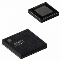
SC16C850SVIBS,115 NXP Semiconductors, SC16C850SVIBS,115 Datasheet - Page 27

SC16C850SVIBS,115
Manufacturer Part Number
SC16C850SVIBS,115
Description
IC UART SGL 1.8V W/FIFO 32-HVQFN
Manufacturer
NXP Semiconductors
Datasheet
1.SC16C850SVIBS151.pdf
(48 pages)
Specifications of SC16C850SVIBS,115
Features
Programmable
Number Of Channels
1, UART
Fifo's
128 Byte
Protocol
RS485
Voltage - Supply
1.8V
With Auto Flow Control
Yes
With Irda Encoder/decoder
Yes
With False Start Bit Detection
Yes
With Modem Control
Yes
With Cmos
Yes
Mounting Type
Surface Mount
Package / Case
32-VFQFN Exposed Pad
Lead Free Status / RoHS Status
Lead free / RoHS Compliant
Other names
935286785115
SC16C850SVIBS-G
SC16C850SVIBS-G
SC16C850SVIBS-G
SC16C850SVIBS-G
NXP Semiconductors
SC16C850SV
Product data sheet
7.8 Modem Status Register (MSR)
Table 20.
This register shares the same address as EFCR register. This is a read-only register and
it provides the current state of the control interface signals from the modem, or other
peripheral device to which the SC16C850SV is connected. Four bits of this register are
used to indicate the changed information. These bits are set to a logic 1 whenever a
control input from the modem changes state. These bits are set to a logic 0 whenever the
CPU reads this register.
When write, the data will be written to EFCR register.
Table 21.
[1]
Bit
0
Bit
6
5
3
1
7
4
2
0
Whenever any MSR bit 3:0 is set to logic 1, a Modem Status Interrupt will be generated.
Symbol Description
LSR[0]
MSR[7]
MSR[6]
MSR[5]
MSR[3]
MSR[1]
Symbol
MSR[4]
MSR[2]
MSR[0]
Line Status Register bits description
Modem Status Register bits description
Single UART with 128-byte FIFOs, IrDA, and XScale VLIO bus interface
Receive data ready.
All information provided in this document is subject to legal disclaimers.
logic 0 = no data in Receive Holding Register or FIFO (normal default condition)
logic 1 = data has been received and is saved in the Receive Holding Register
or FIFO
Description
CD. During normal operation, this bit is the complement of the CD input.
Reading this bit in the loopback mode produces the state of MCR[3] (OP2).
RI. During normal operation, this bit is the complement of the RI input. Reading
this bit in the loopback mode produces the state of MCR[2] (OP1).
DSR. During normal operation, this bit is the complement of the DSR input.
During the loopback mode, this bit is equivalent to MCR[0] (DTR).
CTS. During normal operation, this bit is the complement of the CTS input.
During the loopback mode, this bit is equivalent to MCR[1] (RTS).
CD
RI
DSR
CTS
logic 0 = no CD change (normal default condition)
logic 1 = the CD input to the SC16C850SV has changed state since the last
time it was read. A modem Status Interrupt will be generated.
logic 0 = no RI change (normal default condition)
logic 1 = the RI input to the SC16C850SV has changed from a logic 0 to a
logic 1. A modem Status Interrupt will be generated.
logic 0 = no DSR change (normal default condition)
logic 1 = the DSR input to the SC16C850SV has changed state since the last
time it was read. A modem Status Interrupt will be generated.
logic 0 = no CTS change (normal default condition)
logic 1 = the CTS input to the SC16C850SV has changed state since the last
time it was read. A modem Status Interrupt will be generated.
[1]
[1]
[1]
Rev. 2 — 22 March 2011
[1]
…continued
SC16C850SV
© NXP B.V. 2011. All rights reserved.
27 of 48


