NS16C2752TVS/NOPB National Semiconductor, NS16C2752TVS/NOPB Datasheet - Page 31
NS16C2752TVS/NOPB
Manufacturer Part Number
NS16C2752TVS/NOPB
Description
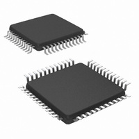
IC UART DUAL 64BYTE 48-TQFP
Manufacturer
National Semiconductor
Datasheet
1.NS16C2552TVSXNOPB.pdf
(44 pages)
Specifications of NS16C2752TVS/NOPB
Features
Programmable
Number Of Channels
2, DUART
Fifo's
64 Byte
Voltage - Supply
2.97 V ~ 5.5 V
With Auto Flow Control
Yes
With Irda Encoder/decoder
Yes
With Modem Control
Yes
Mounting Type
Surface Mount
Package / Case
48-VFQFP
Lead Free Status / RoHS Status
Lead free / RoHS Compliant
Other names
NS16C2752TVS
Available stocks
Company
Part Number
Manufacturer
Quantity
Price
Company:

Part Number:
NS16C2752TVS/NOPB
Manufacturer:
Texas Instruments
Quantity:
10 000


matches the lower trigger level, the UART automatically
transmits Xon1 and Xon2 characters.
Care should be taken when designing the software flow con-
trol section of the driver. In the case where a local UART is
transmitting and the remote UART initiates flow control, an
Xoff character is sent by the remote UART.
Upon receipt the local UART ceases to transmit until such
time as the remote UART FIFO has been drained sufficiently
and it signals that it can accept further data by sending an Xon
character to the local UART.
There is a corner case in which the receipt of an Xoff by the
local UART can occur just after it has sent the last character
of a data transfer and is ready to close the transmission. If in
so doing the driver disables the local UART, it may not receive
the corresponding XON and thus can remain in a flow-con-
trolled state. This will persist even when the UART is re-
enabled for a succeeding transmission creating a lock-up
situation.
To resolve this lock-up issue, the driver should implement a
delay before shutting down the local transmitter at the end of
a data transfer. This delay time should be equal to the trans-
mission time of four characters PLUS the latency required to
drain the RX FIFO on the remote side of the connection. This
will allow the remote modem to send an Xon character and
for it to be received before the local transmitter shuts down.
7.6 SPECIAL CHARACTER DETECT
UART can detect an 8-bit special character if EFR[5]=1. When
special character detect mode is enabled, the UART com-
pares each received character with Xoff2. If a match is found,
Xoff2 is loaded into the FIFO along with the normal received
data and IIR[4] is flagged to logic 1.
The Xon and Xoff word length is programmable between 5
and 8 bits depending on LCR[1:0] with the LSB bit mapped to
bit 0. The same word length is used for special character
comparison.
7.7 SLEEP MODE
To reduce power consumption, NS16C2552/2752 has a per
channel sleep mode when channel is not being used. The
sleep mode requires following conditions to be met:
•
•
•
•
Rx Trigger
TABLE 29. Xon/Xoff SW Flow Control on NS16C2552
TABLE 30. Xon/Xoff SW Flow Control on NS16C2752
Rx Trigge
Sleep mode of the respective channel is enabled (IER[4]
=1).
No pending interrupt for the respective channel (IIR[0]=1).
Divisor is a non-zero value (DLL or DLM != 0x00).
Modem inputs are not toggling (MSR[3:0]=0).
Level
Level
16
56
60
8
14
1
4
8
Activation
Activation
INTR Pin
INTR Pin
16
56
60
14
8
1
4
8
Xoff Char
Xoff Char
Sent
Sent
14
1
4
8
16
56
60
8
Xon Char
Xon Char
Sent
Sent
0
1
4
8
16
56
0
8
31
•
The channel wakes up from sleep mode and returns to normal
operation when one of the following conditions is met:
•
•
•
Following the awakening, the channel can fall back into the
sleep mode when all interrupt conditions are serviced and
cleared. If channel is awakened by the modem line inputs,
reading the MSR resets the line inputs.
Following the awakening, the interrupts from the respective
channel has to be serviced and cleared before re-entering into
the sleep mode. The NS16C2552/2752 sleep mode can be
disabled by IER[4]=0.
7.8 INTERNAL LOOPBACK MODE
NS16C2552 incorporates internal loopback path for design
validation and diagnostic trouble shooting. In the loopback
mode, the transmitted data is looped from the transmit shift
register output to the receive shift register input internally. The
system receives its transmitted data. The loopback mode is
enabled by MCR[4]=1 (Figure 13).
In the loopback mode, Tx pin is held at logic 1 or mark con-
dition while RTS and DTR are de-asserted and CTS, DRS,
CD, and RI inputs are ignored. Note that Rx input must be
held at logic 1 during the loopback test. This is to prevent false
start bit detection upon exiting the loopback mode. RTS and
CTS are disabled during the test.
7.9 DMA OPERATION
LSR[6:5] provide status of the transmit FIFO and LSR[0] pro-
vides the receive FIFO status. User may read the LSR status
bits to initiate and stop data transfers.
More efficient direct memory access (DMA) transfers can be
setup using the RXRDY and TXRDY signals. The DMA trans-
fers are asserted between the CPU cycles and saves CPU
processing bandwidth. In mode 0, (FCR[3]=0), each assertion
of RXRDY and TXRDY will cause a single transfer. Note that
the user should verify the interface to make sure the signaling
is compatible with the DMA controller.
With built-in transmit and receive FIFO buffers it allows data
to be transferred in blocks (mode 1) and it is ideal for more
efficient DMA operation that further saves the CPU process-
ing bandwidth.
To enable the DMA mode 1, FCR[3]=1. The DMA Rx FIFO
reading is controlled by RXRDY. When FIFO data is filled to
the trigger level, RXRDY asserts and the DMA burst transfer
begins removing characters from Rx FIFO. The DMA transfer
stops when Rx FIFO is empty and RXRDY deasserts.
The DMA transmit operation is controlled by TXRDY and is
different between the NS16C2552 and NS16C2752. On the
NS16C2552, the DMA operation is initiated when transmit FI-
FO becomes empty and TXRDY is asserted. The DMA con-
troller fills the Tx FIFO and the filling stops when FIFO is full
and TXRDY is deasserted.
On the NS16C2752, the DMA transfer starts when the Tx FI-
FO empty space exceeds the threshold set in FCR[5:4] and
TXRDY asserts. The transfer stops when Tx FIFO is full and
TXRDY desserts. The threshold setting gives CPU more time
to arbitrate and relinquish bus control to DMA controller pro-
viding higher bus efficiency.
Receiver input is idling at logic 1.
Start bit falling edge (logic 1 to 0) is detected on receiver.
A character is loaded into the THR or Tx FIFO
A state change on any of the modem interface inputs,
DTS, DSR, DCD, and RI.
www.national.com
Related parts for NS16C2752TVS/NOPB
Image
Part Number
Description
Manufacturer
Datasheet
Request
R

Part Number:
Description:
National Semiconductor [8-Bit D/A Converter]
Manufacturer:
National Semiconductor
Datasheet:
Part Number:
Description:
National Semiconductor [Media Coprocessor]
Manufacturer:
National Semiconductor
Datasheet:
Part Number:
Description:
Digitally Controlled Tone and Volume Circuit with Stereo Audio Power Amplifier, Microphone Preamp Stage and National 3D Sound
Manufacturer:
National Semiconductor
Datasheet:
Part Number:
Description:
Digitally Controlled Tone and Volume Circuit with Stereo Audio Power Amplifier, Microphone Preamp Stage and National 3D Sound
Manufacturer:
National Semiconductor
Datasheet:
Part Number:
Description:
AC97 Rev 2 Codec with Sample Rate Conversion and National 3D Sound
Manufacturer:
National Semiconductor
Part Number:
Description:
Manufacturer:
National Semiconductor
Datasheet:
Part Number:
Description:
Manufacturer:
National Semiconductor
Datasheet:
Part Number:
Description:
General Purpose, Low Voltage, Low Power, Rail-to-Rail Output Operational Amplifiers
Manufacturer:
National Semiconductor
Datasheet:
Part Number:
Description:
8-bit 20 MSPS flash A/D converter.
Manufacturer:
National Semiconductor
Datasheet:
Part Number:
Description:
Low Noise Quad Operational Amplifier
Manufacturer:
National Semiconductor
Datasheet:
Part Number:
Description:
Quad Differential Line Receivers
Manufacturer:
National Semiconductor
Datasheet:
Part Number:
Description:
Quad High Speed Trapezoidal? Bus Transceiver
Manufacturer:
National Semiconductor
Datasheet:
Part Number:
Description:
Dual Line Receiver
Manufacturer:
National Semiconductor
Datasheet:
Part Number:
Description:
TTL to 10k ECL Level Translator with Latch
Manufacturer:
National Semiconductor
Datasheet: