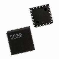
SC16C2552IA44,529 NXP Semiconductors, SC16C2552IA44,529 Datasheet - Page 15

SC16C2552IA44,529
Manufacturer Part Number
SC16C2552IA44,529
Description
IC UART DUAL W/FIFO 44-PLCC
Manufacturer
NXP Semiconductors
Datasheet
1.SC16C2552IA44529.pdf
(38 pages)
Specifications of SC16C2552IA44,529
Features
2 Channels
Number Of Channels
2, DUART
Fifo's
16 Byte
Voltage - Supply
2.5V, 3.3V, 5V
With False Start Bit Detection
Yes
With Modem Control
Yes
With Cmos
Yes
Mounting Type
Surface Mount
Package / Case
44-LCC (J-Lead)
Lead Free Status / RoHS Status
Lead free / RoHS Compliant
Other names
568-1186-5
935270026529
SC16C2552IA44-S
935270026529
SC16C2552IA44-S
Available stocks
Company
Part Number
Manufacturer
Quantity
Price
Company:
Part Number:
SC16C2552IA44,529
Manufacturer:
NXP Semiconductors
Quantity:
10 000
Philips Semiconductors
9397 750 11636
Product data
7.3.1 DMA mode
7.3.2 FIFO mode
7.3 FIFO Control Register (FCR)
This register is used to enable the FIFOs, clear the FIFOs, set the receive FIFO
trigger levels, and select the DMA mode.
Mode 0 (FCR bit 3 = 0):
receive operation, and is similar to the 16C450 mode. Transmit Ready (TXRDY) will
go to a logic 0 whenever an empty transmit space is available in the Transmit Holding
Register (THR). Receive Ready (RXRDY) at the MF pin will go to a logic 0 whenever
the Receive Holding Register (RHR) is loaded with a character and the MF register is
set to the RXRDY mode.
Mode 1 (FCR bit 3 = 1):
transmit interrupt is set when the transmit FIFO has at least one empty location.
TXRDY remains a logic 0 as long as one empty FIFO location is available. The
receive interrupt is set when the receive FIFO fills to the programmed trigger level.
However, the FIFO continues to fill regardless of the programmed level until the FIFO
is full. RXRDY at the MF pin remains a logic 0 as long as the FIFO fill level is above
the programmed trigger level, and the MF register is set to the RXRDY mode.
Table 8:
Bit
7-6
5-4
3
FIFO Control Register bits description
Symbol
FCR[7]
(MSB),
FCR[6]
(LSB)
FCR[5-4]
FCR[3]
Rev. 03 — 20 June 2003
Description
RCVR trigger. These bits are used to set the trigger level for the
receive FIFO interrupt.
An interrupt is generated when the number of characters in the
FIFO equals the programmed trigger level. However, the FIFO will
continue to be loaded until it is full. Refer to
Not used; initialized to logic 0.
DMA mode select.
Transmit operation in mode ‘0’: When the SC16C2552 is in the
16C450 mode (FIFOs disabled; FCR[0] = logic 0) or in the FIFO
mode (FIFOs enabled; FCR[0] = logic 1; FCR[3] = logic 0), and
when there are no characters in the transmit FIFO or transmit
holding register, the TXRDY pin will be a logic 0. Once active, the
TXRDY pin will go to a logic 1 after the first character is loaded into
the transmit holding register.
Receive operation in mode ‘0’: When the SC16C2552 is in
16C450 mode, or in the FIFO mode (FCR[0] = logic 1;
FCR[3] = logic 0) and there is at least one character in the receive
FIFO, the RXRDY signal at the MF pin will be a logic 0. Once
active, the RXRDY signal at the MF pin will go to a logic 1 when
there are no more characters in the receiver. NOTE: The AFR
register must be set to the RXRDY mode prior to any possible
reading of the RXRDY signal.
Set and enable the interrupt for each single transmit or
Set and enable the interrupt in a block mode operation. The
Logic 0 = Set DMA mode ‘0’ (normal default condition).
Logic 1 = Set DMA mode ‘1’
Dual UART with 16-byte transmit and receive FIFOs
© Koninklijke Philips Electronics N.V. 2003. All rights reserved.
SC16C2552
Table
9.
15 of 38


