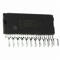
TDA8920CJ/N1,112 NXP Semiconductors, TDA8920CJ/N1,112 Datasheet - Page 16

TDA8920CJ/N1,112
Manufacturer Part Number
TDA8920CJ/N1,112
Description
IC AMP AUDIO PWR 220W 23SIL
Manufacturer
NXP Semiconductors
Type
Class Dr
Datasheet
1.TDA8920CJN1112.pdf
(39 pages)
Specifications of TDA8920CJ/N1,112
Output Type
1-Channel (Mono) or 2-Channel (Stereo)
Package / Case
23-SIL (Bent and Staggered Leads)
Max Output Power X Channels @ Load
220W x 1 @ 8 Ohm; 125W x 2 @ 4 Ohm
Voltage - Supply
±12.5 V ~ 32.5 V
Features
Depop, Differential Inputs, Mute, Short-Circuit and Thermal Protection, Standby
Mounting Type
Through Hole
Product
Class-D
Output Power
210 W
Available Set Gain
36 dB
Common Mode Rejection Ratio (min)
75 dB
Thd Plus Noise
0.05 %
Maximum Operating Temperature
+ 85 C
Mounting Style
Through Hole
Audio Load Resistance
8 Ohms
Dual Supply Voltage
+/- 30 V
Input Signal Type
Differential
Minimum Operating Temperature
- 40 C
Output Signal Type
Differential, Single
Supply Type
Dual
Lead Free Status / RoHS Status
Lead free / RoHS Compliant
Other names
568-4784-5
935281808112
TDA8920CJ/N1
TDA8920CJ/N1,112
TDA8920CJ/N1
935281808112
TDA8920CJ/N1
TDA8920CJ/N1,112
TDA8920CJ/N1
NXP Semiconductors
Table 11.
V
[1]
[2]
[3]
[4]
[5]
[6]
[7]
TDA8920C_2
Product data sheet
Symbol
P
THD
G
SVRR
Z
V
CMRR
P
i
mute
o
n(o)
v(cl)
= 30 V; R
R
Output power is measured indirectly; based on R
THD measured between 22 Hz and 20 kHz, using AES17 20 kHz brick wall filter; max. limit is guaranteed but may not be 100 % tested.
V
22 Hz to 20 kHz, using an AES17 20 kHz brick wall filter; low noise due to BD modulation.
22 Hz to 20 kHz, using an AES17 20 kHz brick wall filter.
V
ripple
i
sL
= V
is the series resistance of the low-pass LC filter inductor used in the application.
i(max)
= V
Parameter
output power
total harmonic distortion
closed-loop voltage gain
supply voltage ripple rejection
input impedance
output noise voltage
mute attenuation
common mode rejection ratio
Dynamic characteristics
ripple(max)
L
= 1 V (RMS); f
= 8 ; f
12.3 Mono BTL application characteristics
= 2 V (p-p).
i
= 1 kHz; f
i
= 1 kHz.
osc
= 345 kHz; R
DSon
sL
Rev. 02 — 11 June 2009
[1]
measurement; see
< 0.1
Conditions
T
(see
P
P
between pin VDDPn and SGND
between pin VSSPn and SGND
measured between one of the input
pins and SGND
Operating mode; R
Mute mode
f
V
i
j
o
o
i(CM)
= 1 kHz; V
THD = 0.5 %; R
THD = 10 %; R
Operating mode; f
Operating mode; f
Mute mode; f
Standby mode; f
Operating mode; f
Operating mode; f
Mute mode; f
Standby mode; f
= 85 C; L
= 1 W; f
= 1 W; f
Figure
; T
= 1 V (RMS)
amb
i
i
= 1 kHz
= 6 kHz
= 25 C; unless otherwise specified.
10)
i
LC
Section
= 2 V (RMS)
= 22 H; C
i
i
= 100 Hz
= 100 Hz
L
L
i
i
= 8
s
= 100 Hz
= 100 Hz
= 8
13.3.
i
i
i
i
= 0
= 100 Hz
= 1 kHz
= 100 Hz
= 1 kHz
LC
2
= 680 nF
110 W class-D power amplifier
[2]
[3]
[3]
[4]
[4]
[4]
[4]
[4]
[4]
[4]
[4]
[5]
[6]
[7]
TDA8920C
Min Typ Max Unit
-
-
-
-
-
-
-
-
-
-
-
-
-
45
-
-
-
-
© NXP B.V. 2009. All rights reserved.
170
220
0.05 -
0.05 -
36
80
80
95
120
75
75
90
130
63
190
45
75
75
-
-
-
-
-
-
-
-
-
-
-
-
-
-
-
-
16 of 39
W
W
%
%
dB
dB
dB
dB
dB
dB
dB
dB
dB
k
dB
dB
V
V


