LM49450SQ/NOPB National Semiconductor, LM49450SQ/NOPB Datasheet
LM49450SQ/NOPB
Specifications of LM49450SQ/NOPB
LM49450SQ
LM49450SQTR
Available stocks


Related parts for LM49450SQ/NOPB

LM49450SQ/NOPB Summary of contents
Page 1
... Quiescent Power Supply Current Line Inputs: Speaker Mode at LSV = 3.6V DD Headphone Mode at HPV = 2.5V DD Boomer® registered trademark of National Semiconductor Corporation. © 2008 National Semiconductor Corporation ■ Output Power/Channel Speaker at LSV = 4Ω, THD 8Ω, THD+N R ...
Page 2
Typical Application www.national.com 2 ...
Page 3
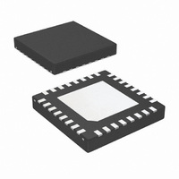
Connection Diagrams SQ Package 5mm x 5mm x 0.8mm Top View Order Number LM49450SQ See NS Package Number SQA32A SQ Marking 5mm x 5mm x 0.8mm 30045533 Top View Logo U - Wafer Fab Code Z - ...
Page 4
... Absolute Maximum Ratings If Military/Aerospace specified devices are required, please contact the National Semiconductor Sales Office/ Distributors for availability and specifications. Supply Voltage (Note 1) Storage Temperature Input Voltage Power Dissipation (Note 3) ESD Susceptibility(Note 4) ESD Susceptibility (Note 5) Junction Temperature (T ) JMAX Thermal Resistance Electrical Characteristics V ...
Page 5
Symbol Parameter SNR Signal to Noise Ratio A Digitally Controlled Gain Level V Mute Mute Attenuation Channel-to-Channel Gain ΔA CH-CH Matching ε Output Noise OS t Turn-On Time ON t Turn-Off Time OFF HEADPHONE AMPLIFIERS (Speaker Amplifiers Disabled, HPS = ...
Page 6
Symbol Parameter A Digitally Controlled Gain Level V Mute Mute Attenuation Channel-to-Channel Gain ΔA CH-CH Matching ε Output Noise OS Full-Scale Headphone Amplifier V OUT_FS Output Voltage t Turn-On Time ON t Turn-Off Time OFF HEADPHONE SENSE INPUT (HPS) V ...
Page 7
Symbol Parameter η Efficiency Xtalk Crosstalk SNR Signal to Noise Ratio A Digitally Controlled Gain Level V Mute Mute Attenuation Channel-to-Channel Gain ΔA CH-CH Matching ε Output Noise OS t Turn-On Time ON t Turn-Off Time OFF Timing Characteristics 8Ω, ...
Page 8
Symbol Parameter Clock Low Time 2 3 Clock High Time Setup Time for a Repeated 4 START Condition Data Hold Time 5 6 Data Setup Time 7 Rise Time of SDA and SCL Fall Time of SDA and SCL 8 ...
Page 9
Pin Descriptions Pin Name 1 C1P 2 CPGND 3 SDA 4 DGND S_WS S_SDI S_CLK 8 MCLK 9 SCL IOV DD 12 GND 13 REF 14 INR ...
Page 10
Typical Performance Characteristics THD+N vs Frequency V = 3.0V 50mW OUT DAC Input, Internal Reference, Speaker Mode THD+N vs Frequency V = 3.0V 50mW OUT DAC Input, External Reference, Speaker Mode THD+N ...
Page 11
THD+N vs Frequency = 4Ω 3.6V 100mW OUT L DAC Input, Internal Reference, Speaker Mode THD+N vs Frequency = 8Ω 3.6V 100mW OUT L Analog Input, Speaker Mode ...
Page 12
THD+N vs Frequency V = 5.0V 750mW OUT DAC Input, Internal Reference, Speaker Mode THD+N vs Frequency V = 5.0V 800mW OUT DAC Input, Internal Reference, Speaker Mode THD+N vs Frequency V ...
Page 13
THD+N vs Frequency HPV = 2.0V 10mW OUT L DAC Input, Internal Reference, Headphone Mode THD+N vs Frequency HPV = 2.0V 15mW OUT L DAC Input, Internal Reference, Headphone Mode THD+N vs ...
Page 14
THD+N vs Frequency HPV = 2.0V 15mW OUT DAC Input, External Reference, Headphone Mode THD+N vs Frequency HPV = 2.0V 10mW OUT Analog Input, Headphone Mode THD+N vs Frequency HPV = 2.5V, ...
Page 15
THD+N vs Output Power = 4Ω 1kHz A = 12dB DAC Input, Internal Reference, Speaker Mode THD+N vs Output Power = 8Ω 1kHz A = 12dB DAC Input, Internal Reference, ...
Page 16
THD+N vs Output Power = 16Ω 1kHz A = 9dB DAC Input, Internal Reference, Headphone Mode THD+N vs Output Power = 32Ω 1kHz A = 9dB DAC Input, External Reference, ...
Page 17
PSRR vs Frequency V = 3.6V 200mV , R DD RIPPLE P-P DAC Input, External Reference, Speaker Mode PSRR vs Frequency HPV = 2.5V 200mV , R DD RIPPLE P-P DAC Input, Internal Reference, Headphone Mode ...
Page 18
Power Dissipation vs Output Power = 4Ω 1kHz, Speaker Mode R L Power Dissipation vs Output Power = 16Ω 1kHz, Headphone Mode R L Output Power vs Supply Voltage = 4Ω 1kHz, Speaker Mode ...
Page 19
Output Power vs Supply Voltage = 16Ω 1kHz, Headphone Mode R L Output Noise vs Frequency = 8Ω 3.6V DAC Input, Internal Reference, Speaker Mode Output Noise vs Frequency = 32Ω ...
Page 20
Crosstalk vs Frequency V = 3.6V RIPPLE Analog Input, Speaker Mode www.national.com = 8Ω P-P L 300455e9 20 Crosstalk vs Frequency = 8Ω 2.5V RIPPLE P-P ...
Page 21
Application Information I2C COMPATIBLE INTERFACE The LM49450 is controlled through an I interface that consists of a serial data line (SDA) and a serial clock (SCL). The clock line is uni-directional. The data line is bi-directional (open collector). The LM49450 ...
Page 22
ACK bit. Following the acknowledgement of the register data word, the master issues a STOP bit, allowing SDA to go high while SDA is high DATA FORMAT The LM49450 supports three formats: Normal ...
Page 23
Fixed Frequency Mode The LM49450 features two modulation schemes, a fixed fre- quency mode and a spread spectrum mode. Select the fixed frequency mode by setting the SS bit (B3) in the Mode Control Register (0x00h fixed ...
Page 24
External Reference The LM49450 can be used with an external reference. Dis- able the internal reference by setting bit B7 of the Mode Control Register (0x00h This allows an external refer- ence voltage to be applied to REF. ...
Page 25
25 www.national.com ...
Page 26
MODE CONTROL REGISTER (0x00h) Default value is 0x00h. Bit Name B7 EXT_REF DAC_MODE_1 (B6) B6:B5 DAC_MODE_0 (B5) B4 COMP MUTE B0 ENABLE CLOCK CONTROL REGISTER (0x01h) Default value is 0x00h. Bit Name B7 DAC_DITHER_OFF B6 DAC_DITHER_ON B5 ...
Page 27
CLK NETWORK LM49450 Clock Structure The MCLK input is first divided by the R divider to product the clock at point B; this is then decoded according to the DAC_MODE to produce a signal which goes to both the DAC ...
Page 28
CHARGE PUMP CLOCK REGISTER (0x02h) The charge pump clock register sets the charge pump fre- quency derived from MCLK when the LM49450 is in DAC mode. Default value is for register 02h is 0x49h. Bit Name CPDIV_7 B7 B6 (B7) ...
Page 29
MCLK (MHZ) 11.025 12 TABLE 9. Typical CP_DIV Values for DAC Mode 01 MCLK (MHZ) 2.048 2.8224 3.072 4.096 5.6448 6.144 8.192 11.2896 12.288 TABLE 10. Typical CP_DIV Values for DAC Mode 10 MCLK (MHZ) 11.2896 12.288 TABLE 11. Typical ...
Page 30
Bit Name I2S_WORD_ORD B2 ER I2S_MODE_1 (B1) B1:B0 I2S_MODE_0 (B0) I2S CLOCK REGISTER (0x04h) Default value is 0x00h. Bit Name I2S_CLK_3 (B7) 0 I2S_CLK_2 0 (B6) B7:B4 0 I2S_CLK_1 0 (B5) I2S_CLK_0 1 (B4) 1 ...
Page 31
HEADPHONE 3D CONFIGURATION REGISTER (0x05h) Default value is 0x00h. TABLE 14. Headphone 3D Configuration Register Bit Name B7 RESERVED B6 HP_3DATTN HP_3DFREQ_1 (B5) B5:B4 HP_3DFREQ_0 (B4) HP_3DFREQ_1 (B3) B3:B2 HP_3DFREQ_0 (B2) B1 HP_3D B0 HP_3DEN LOUDSPEAKER 3D CONFIGURATION REGISTER (0x06h) ...
Page 32
HEADPHONE VOLUME CONTROL REGISTER (0x07h) Default value is 0x00h. Bit Name B7:B5 RESERVED HP4 (B4) HP3 (B3) B4:B0 HP2 (B2) HP1 (B1) HP0 (B0) VOLUME HP4 STEP ...
Page 33
LOUDSPEAKER VOLUME CONTROL REGISTER (0x08h) Default value is 0x00h. TABLE 17. Loudspeaker Volume Control Register Bit Name B7:B5 RESERVED LS4 (B4) LS3 (B3) B4:B0 LS2 (B2) LS1 (B1) LS0 (B0) VOLUME LS4 STEP ...
Page 34
DAC COMPENSATION FILTER REGISTERS (0x09h to 0x0Eh) DAC Compensation Filter The LM49450 DAC features a 5 band FIR filter that can be used as an equalizer for the digital audio path. Registers 0x09h, 0x0Ah, 0x0Bh, 0x0Ch, 0x0Dh, and 0x0Eh provide ...
Page 35
PCB Layout Guidelines Minimize trace impedance of the power, ground and all output traces for optimum performance. Voltage loss due to trace resistance between the LM49450 and the load results in de- creased output power and efficiency. Trace resistance be- ...
Page 36
Revision Table Rev Date 1.0 12/18/07 1.01 09/26/08 www.national.com Description Initial release. Corrected the package drawing. 36 ...
Page 37
Physical Dimensions inches (millimeters) unless otherwise noted 32 Lead LLP Order Number LM49450SQ NS Package Number SQA32A 37 www.national.com ...
Page 38
... For more National Semiconductor product information and proven design tools, visit the following Web sites at: Products Amplifiers www.national.com/amplifiers Audio www.national.com/audio Clock Conditioners www.national.com/timing Data Converters www.national.com/adc Displays www.national.com/displays Ethernet www.national.com/ethernet Interface www.national.com/interface LVDS www.national.com/lvds Power Management www.national.com/power Switching Regulators www.national.com/switchers LDOs www ...