LM49450SQ/NOPB National Semiconductor, LM49450SQ/NOPB Datasheet - Page 21
LM49450SQ/NOPB
Manufacturer Part Number
LM49450SQ/NOPB
Description
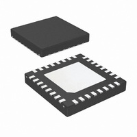
IC AUDIO SUBSYSTEM 2.5W D 32LLP
Manufacturer
National Semiconductor
Series
Boomer®r
Type
Class Dr
Datasheet
1.LM49450SQNOPB.pdf
(38 pages)
Specifications of LM49450SQ/NOPB
Output Type
2-Channel (Stereo) with Stereo Headphones
Max Output Power X Channels @ Load
2.5W x 2 @ 4 Ohm
Voltage - Supply
2.7 V ~ 5.5 V
Features
3D, DAC, Depop, I²C, I²S, Mute, Short-Circuit and Thermal Protection, Shutdown, Volume Control
Mounting Type
Surface Mount
Package / Case
32-LLP
Amplifier Class
D
No. Of Channels
2
Output Power
1.2W
Supply Voltage Range
2.7V To 5.5V
Load Impedance
8ohm
Operating Temperature Range
-40°C To +85°C
Amplifier Case Style
LLP
Rohs Compliant
Yes
For Use With
LM49450SQEVAL - BOARD EVAL FOR LM49450
Lead Free Status / RoHS Status
Lead free / RoHS Compliant
Other names
LM49450SQ
LM49450SQ
LM49450SQTR
LM49450SQ
LM49450SQTR
Available stocks
Company
Part Number
Manufacturer
Quantity
Price

Part Number:
LM49450SQ/NOPB
Manufacturer:
TI/德州仪器
Quantity:
20 000


Application Information
I2C COMPATIBLE INTERFACE
The LM49450 is controlled through an I
interface that consists of a serial data line (SDA) and a serial
clock (SCL). The clock line is uni-directional. The data line is
bi-directional (open collector). The LM49450 and the master
can communicate at clock rates up to 400kHz. Figure 2 shows
the I
be stable during the HIGH period of SCL. The LM49450 is a
BUS FORMAT
The I
the transition of SDA from HIGH to LOW while SDA is HIGH,
is generated, altering all devices on the bus that a device ad-
dress is being written to the bus.
The 7-bit device address is written to the bus, most significant
bit (MSB) first, followed by the R/W bit (R/W = 0 indicates the
master is writing to the LM49450, R/W = 1 indicates the mas-
ter wants to read data from the LM49450). The data is latched
in on the rising edge of the clock. Each address bit must be
stable while SDA is HIGH. After the last address bit is trans-
2
2
C interface timing diagram. Data on the SDA line must
C bus format is shown in Figure 4. The START signal,
2
C compatible serial
FIGURE 3. START and STOP Diagram
FIGURE 4. Example I2C Write Cycle
FIGURE 2. I2C Timing Diagram
21
transmit/receive slave-only device, reliant upon the master to
generate the SCL signal. Each transmission sequence is
framed by a START condition and a STOP condition (Figure
3). Each data word, register address and register data, trans-
mitted over the bus is 8 bits long as is always followed by and
acknowledge pulse (Figure 3). The LM49450 device address
is 1111101.
mitted, the master device releases SDA, during which time,
an acknowledge clock pulse is generated by the slave device.
If the LM49450 receives the correct address, the device pulls
the SDA line low, generating and acknowledge bit (ACK).
Once the master device registers the ACK bit, the 8-bit reg-
ister address word is sent. Each data bit should be stable
while SCL is HIGH. After the 8-bit register address is sent, the
LM49450 sends another ACK bit. Following the acknowl-
edgement of the register address, the 8-bit register data word
is sent. Each data bit should be stable while SCL is HIGH.
After the 8-bit register data is sent, the LM49450 sends an-
300455h9
300455h8
www.national.com
300455b0
Related parts for LM49450SQ/NOPB
Image
Part Number
Description
Manufacturer
Datasheet
Request
R

Part Number:
Description:
National Semiconductor [8-Bit D/A Converter]
Manufacturer:
National Semiconductor
Datasheet:
Part Number:
Description:
National Semiconductor [Media Coprocessor]
Manufacturer:
National Semiconductor
Datasheet:
Part Number:
Description:
Digitally Controlled Tone and Volume Circuit with Stereo Audio Power Amplifier, Microphone Preamp Stage and National 3D Sound
Manufacturer:
National Semiconductor
Datasheet:
Part Number:
Description:
Digitally Controlled Tone and Volume Circuit with Stereo Audio Power Amplifier, Microphone Preamp Stage and National 3D Sound
Manufacturer:
National Semiconductor
Datasheet:
Part Number:
Description:
AC97 Rev 2 Codec with Sample Rate Conversion and National 3D Sound
Manufacturer:
National Semiconductor
Part Number:
Description:
Manufacturer:
National Semiconductor
Datasheet:
Part Number:
Description:
Manufacturer:
National Semiconductor
Datasheet:
Part Number:
Description:
General Purpose, Low Voltage, Low Power, Rail-to-Rail Output Operational Amplifiers
Manufacturer:
National Semiconductor
Datasheet:
Part Number:
Description:
8-bit 20 MSPS flash A/D converter.
Manufacturer:
National Semiconductor
Datasheet:
Part Number:
Description:
Low Noise Quad Operational Amplifier
Manufacturer:
National Semiconductor
Datasheet:
Part Number:
Description:
Quad Differential Line Receivers
Manufacturer:
National Semiconductor
Datasheet:
Part Number:
Description:
Quad High Speed Trapezoidal? Bus Transceiver
Manufacturer:
National Semiconductor
Datasheet:
Part Number:
Description:
Dual Line Receiver
Manufacturer:
National Semiconductor
Datasheet:
Part Number:
Description:
TTL to 10k ECL Level Translator with Latch
Manufacturer:
National Semiconductor
Datasheet: