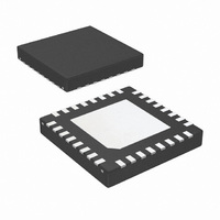
LM49450SQ/NOPB National Semiconductor, LM49450SQ/NOPB Datasheet - Page 24

LM49450SQ/NOPB
Manufacturer Part Number
LM49450SQ/NOPB
Description
IC AUDIO SUBSYSTEM 2.5W D 32LLP
Manufacturer
National Semiconductor
Series
Boomer®r
Type
Class Dr
Datasheet
1.LM49450SQNOPB.pdf
(38 pages)
Specifications of LM49450SQ/NOPB
Output Type
2-Channel (Stereo) with Stereo Headphones
Max Output Power X Channels @ Load
2.5W x 2 @ 4 Ohm
Voltage - Supply
2.7 V ~ 5.5 V
Features
3D, DAC, Depop, I²C, I²S, Mute, Short-Circuit and Thermal Protection, Shutdown, Volume Control
Mounting Type
Surface Mount
Package / Case
32-LLP
Amplifier Class
D
No. Of Channels
2
Output Power
1.2W
Supply Voltage Range
2.7V To 5.5V
Load Impedance
8ohm
Operating Temperature Range
-40°C To +85°C
Amplifier Case Style
LLP
Rohs Compliant
Yes
For Use With
LM49450SQEVAL - BOARD EVAL FOR LM49450
Lead Free Status / RoHS Status
Lead free / RoHS Compliant
Other names
LM49450SQ
LM49450SQ
LM49450SQTR
LM49450SQ
LM49450SQTR
Available stocks
Company
Part Number
Manufacturer
Quantity
Price
Part Number:
LM49450SQ/NOPB
Manufacturer:
TI/德州仪器
Quantity:
20 000
www.national.com
External Reference
The LM49450 can be used with an external reference. Dis-
able the internal reference by setting bit B7 of the Mode
Control Register (0x00h) to 1. This allows an external refer-
ence voltage to be applied to REF. For proper operation, do
not allow the V
Low Power Shutdown
The LM49450 features an I
mode that disables the entire device, reducing quiescent cur-
rent consumption to 0.05µA (digital + analog current). Set bit
B0 in the mode control register (0x00h) to 0 to disable the
device. Set B0 to 1 to enable the device.
I2S CLOCK CONTROL
The LM49450 features the ability to derive multiple clock sig-
nals, including the DAC clock, I
in master mode, and the charge pump oscillator frequency,
from the MCLK input.
DAC Clock Divider (RDIV)
Bits B5-B0 in the CLOCK CONTROL register (0x01h) are the
RDIV bits that set the DAC clock divider ratio. The DAC clock
derived from MCLK needs to match the DAC sampling rate.
For example, with f
REF
to exceed V
MCLK
= 12.288MHz and a 64*f
2
C selectable low power shutdown
2
DD
S clock and word select clock
.
S
oversam-
24
pling ratio (f
In this case, set the RDIV ratio to divide by 2. In other in-
stances, there may not be a suitable divider ratio for a given
sampling rate and MCLK frequency. In this case, f
need to be altered. See the Clock Control Register section for
more information.
I
In I
register (0x04h) can be used to set the I
frequency. In I2S clock master mode, bits B7-B4 of the I2S
CLOCK CONTROL register, the I2S_CLK bits, set the I
clock divider ratio. The LM49450 derives the I
DAC clock based on the ratio set by the I2S_CLK bits. The
I
In I
CLOCK CONTROL register set the bit length per data word
of the I
Charge Pump Clock Divider (CPDIV)
The ground referenced headphone amplifiers charge pump
derives its clock from MCLK. Bits B7-B0 of the CHARGE
PUMP CLOCK register (0x02h) set the charge pump clock
divider ratio. See the Charge Pump Clock Register section for
more information.
2
2
S WS Clock Dividers (I2S_CLK, WS_CLK)
S clock is output on I
2
2
S master mode, the LM49450 I2S CLOCK CONTROL
S master mode, bits B3 and B2 (I2S_WS) of the I2S
2
S WS.
S
= 48kHz), the DAC requires a 6.144MHz clock.
2
S_CLK.
2
S clock and WS clock
2
S clock from
MCLK
may
2
S


