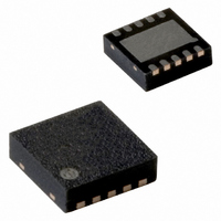
SA58672TK,138 NXP Semiconductors, SA58672TK,138 Datasheet - Page 14

SA58672TK,138
Manufacturer Part Number
SA58672TK,138
Description
IC AMP AUDIO 3W MONO D 10HVSON
Manufacturer
NXP Semiconductors
Type
Class Dr
Datasheet
1.SA58672UK027.pdf
(27 pages)
Specifications of SA58672TK,138
Output Type
1-Channel (Mono)
Package / Case
10-HVSON
Max Output Power X Channels @ Load
3W x 1 @ 4 Ohm
Voltage - Supply
2 V ~ 5.5 V
Features
Differential Inputs, Short-Circuit and Thermal Protection, Shutdown
Mounting Type
Surface Mount
Product
Class-D
Output Power
3 W
Common Mode Rejection Ratio (min)
69 dB
Thd Plus Noise
0.08 %
Operating Supply Voltage
3 V, 5 V
Supply Current
3.4 mA
Maximum Power Dissipation
3.12 mW
Maximum Operating Temperature
+ 85 C
Mounting Style
SMD/SMT
Audio Load Resistance
8 Ohms
Input Signal Type
Differential
Minimum Operating Temperature
- 40 C
Output Signal Type
Differential, Single
Supply Type
Single
Supply Voltage (max)
5.5 V
Supply Voltage (min)
2 V
Lead Free Status / RoHS Status
Lead free / RoHS Compliant
Lead Free Status / RoHS Status
Lead free / RoHS Compliant, Lead free / RoHS Compliant
Other names
935286769138
SA58672TK-T
SA58672TK-T
SA58672TK-T
SA58672TK-T
NXP Semiconductors
SA58672_4
Product data sheet
11.4 PCB layout considerations
11.5 Evaluation demo board
For a required 3 dB cut-off frequency,
The input signal may be DC-coupled, but not using input coupling capacitors may
increase the output offset voltage.
The component location is very important for performance of the SA58672. Place all
external components very close to the device. Placing decoupling capacitors directly at
the power supply pins increases efficiency because the resistance and inductance in the
trace between the device power supply pins and the decoupling capacitor causes a loss in
power efficiency.
The trace width and routing are also very important for power output and noise
considerations.
For high current terminals (PVDD, PGND and audio output), the trace widths should be
maximized to ensure proper performance and output power. Use at least 500 m wide
traces.
For the input pins (INP, INM), the traces must be symmetrical and run side-by-side to
maximize common-mode cancellation.
The SA58672 evaluation demo board schematic is shown in
demo board is available and it may be used for either differential or single-ended (SE)
input configuration. A component position on the PCB is provided to AC ground one of the
inputs using a 0
DC level as driven input. If the input is driven from an iPOD or MP3 player, the undriven
input is AC grounded; however, if driven from a CODEC, the undriven input is AC
decoupled to the same level as the CODEC output. Usually, a V
CODEC.
C
i
=
------------------------------------- -
2
R
i
1
f
–
3dB
chip resistor. When driving SE, the undriven input must be at the same
Rev. 04 — 8 June 2009
Equation 3
is used to determine C
3.0 W mono class-D audio amplifier
Figure
ref
is provided on the
14. An evaluation
SA58672
© NXP B.V. 2009. All rights reserved.
i
:
14 of 27
(3)


