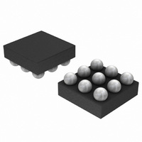
NCP2820AFCT2G ON Semiconductor, NCP2820AFCT2G Datasheet - Page 13

NCP2820AFCT2G
Manufacturer Part Number
NCP2820AFCT2G
Description
IC PWR AMP AUDIO 2.65W D 9-CSP
Manufacturer
ON Semiconductor
Type
Class Dr
Datasheet
1.NCP2820FCT1G.pdf
(22 pages)
Specifications of NCP2820AFCT2G
Output Type
1-Channel (Mono)
Max Output Power X Channels @ Load
2.65W x 1 @ 4 Ohm
Voltage - Supply
2.5 V ~ 5.5 V
Features
Depop, Differential Inputs, Short-Circuit and Thermal Protection, Shutdown
Mounting Type
Surface Mount
Package / Case
9-FlipChip
Operational Class
Class-D
Audio Amplifier Output Configuration
1-Channel Mono
Output Power (typ)
2.63x1@4OhmW
Audio Amplifier Function
Speaker
Total Harmonic Distortion
0.05@8Ohm@0.25W%
Single Supply Voltage (typ)
3/5V
Dual Supply Voltage (typ)
Not RequiredV
Power Supply Requirement
Single
Rail/rail I/o Type
No
Power Supply Rejection Ratio
65dB
Single Supply Voltage (min)
2.5V
Single Supply Voltage (max)
5.5V
Dual Supply Voltage (min)
Not RequiredV
Dual Supply Voltage (max)
Not RequiredV
Operating Temp Range
-40C to 85C
Operating Temperature Classification
Industrial
Mounting
Surface Mount
Pin Count
9
Lead Free Status / RoHS Status
Lead free / RoHS Compliant
Available stocks
Company
Part Number
Manufacturer
Quantity
Price
Company:
Part Number:
NCP2820AFCT2G
Manufacturer:
ON Semiconductor
Quantity:
1 300
Part Number:
NCP2820AFCT2G
Manufacturer:
ON/安森美
Quantity:
20 000
Detailed Description
analog pre-amplifier, a pulse width modulator and an
H-bridge CMOS power stage. The first stage is externally
configurable with gain-setting resistor R
fixed feedback resistor R
the ratios of these resistors) and the other stage is fixed. The
load is driven differentially through two output stages.
the analog audio input signal. The human ear is a band pass
filter regarding acoustic waveforms, the typical values of
which are 20 Hz and 20 kHz. Thus, the user will hear only
the amplified audio input signal within the frequency range.
The switching frequency and its harmonics are fully filtered.
The inductive parasitic element of the loudspeaker helps to
guarantee a superior distortion value.
Power Amplifier
have been designed to deliver the output power of the
specifications without clipping. The channel resistance
(R
Turn On and Turn Off Transitions in the 9 Pin
Flip-Chip Package (NCP2820)
transition, the output power in the load must not be
established or cutoff suddenly. When a logic high is applied
to the shutdown pin, the internal biasing voltage rises
quickly and, 4 ms later, once the output DC level is around
the common mode voltage, the gain is established slowly
(5.0 ms). This method to turn on the device is optimized in
terms of rejection of “pop and click” noises. Thus, the total
turn on time to get full power to the load is 9 ms (typical).
a logic low on the shutdown pin. No power is delivered to the
load 5 ms after a falling edge on the shutdown pin. Due to
The basic structure of the NCP2820 is composed of one
The differential PWM output signal is a digital image of
The output PMOS and NMOS transistors of the amplifier
In order to eliminate “pop and click” noises during
The device has the same behavior when it is turned-off by
on
10
11
) of the NMOS and PMOS transistors is typically 0.4 W.
9
8
7
6
2.5
T
T
T
A
A
A
= +85°C
= +25°C
= -40°C
Figure 33. Turn on Time
3.5
POWER SUPPLY (V)
f
(the closed-loop gain is fixed by
4.5
i
and the internal
DESCRIPTION INFORMATION
NCP2820 Series
http://onsemi.com
5.5
13
the fast turn on and off times, the shutdown signal can be
used as a mute signal as well.
Turn On and Turn Off Transitions in the 9 Pin
Flip-Chip Package (NCP2820)
as the NCP2820. Only the timing is different with 1 ms for
the turn on and 500 ms for the turn off sequence.
Turn On and Turn Off Transitions in the UDFN8
established instantaneously after the rising edge on the
shutdown pin. The audio is also suddenly cut once a low
level is sent to the amplifier. This way to turn on and off the
device in a very fast way also prevents from “pop & click”
noise.
Shutdown Function
signal is low. During the shutdown mode, the DC quiescent
current of the circuit does not exceed 1.5 mA.
Current Breaker Circuit
an average current in the load of 820 mA.
load if a short-circuit occurs, a current breaker cell shuts
down the output stage. The current in the four output MOS
transistors are real-time controlled, and if one current
exceeds the threshold set to 1.5 A, the MOS transistor is
opened and the current is reduced to zero. As soon as the
short-circuit is removed, the circuit is able to deliver the
expected output power.
completely turns off the load, it minimizes the risk of the
chip overheating which could occur if a soft current limiting
circuit was used.
In the case of the NCP2820A, the sequences are the same
In the case of the UDFN8 package, the audio signal is
The device enters shutdown mode when the shutdown
The maximum output power of the circuit corresponds to
In order to limit the excessive power dissipation in the
This patented structure protects the NCP2820. Since it
8
7
6
5
4
2.5
T
A
= +85°C
Figure 34. Turn off Time
T
3.5
A
POWER SUPPLY (V)
= +25°C
T
A
= -40°C
4.5
5.5


