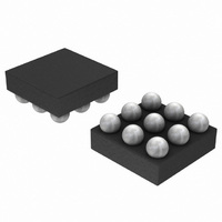
NCP2820AFCT2G ON Semiconductor, NCP2820AFCT2G Datasheet - Page 14

NCP2820AFCT2G
Manufacturer Part Number
NCP2820AFCT2G
Description
IC PWR AMP AUDIO 2.65W D 9-CSP
Manufacturer
ON Semiconductor
Type
Class Dr
Datasheet
1.NCP2820FCT1G.pdf
(22 pages)
Specifications of NCP2820AFCT2G
Output Type
1-Channel (Mono)
Max Output Power X Channels @ Load
2.65W x 1 @ 4 Ohm
Voltage - Supply
2.5 V ~ 5.5 V
Features
Depop, Differential Inputs, Short-Circuit and Thermal Protection, Shutdown
Mounting Type
Surface Mount
Package / Case
9-FlipChip
Operational Class
Class-D
Audio Amplifier Output Configuration
1-Channel Mono
Output Power (typ)
2.63x1@4OhmW
Audio Amplifier Function
Speaker
Total Harmonic Distortion
0.05@8Ohm@0.25W%
Single Supply Voltage (typ)
3/5V
Dual Supply Voltage (typ)
Not RequiredV
Power Supply Requirement
Single
Rail/rail I/o Type
No
Power Supply Rejection Ratio
65dB
Single Supply Voltage (min)
2.5V
Single Supply Voltage (max)
5.5V
Dual Supply Voltage (min)
Not RequiredV
Dual Supply Voltage (max)
Not RequiredV
Operating Temp Range
-40C to 85C
Operating Temperature Classification
Industrial
Mounting
Surface Mount
Pin Count
9
Lead Free Status / RoHS Status
Lead free / RoHS Compliant
Available stocks
Company
Part Number
Manufacturer
Quantity
Price
Company:
Part Number:
NCP2820AFCT2G
Manufacturer:
ON Semiconductor
Quantity:
1 300
Part Number:
NCP2820AFCT2G
Manufacturer:
ON/安森美
Quantity:
20 000
NCP2820 PWM Modulation Scheme
output switching from 0 to the supply voltage. If V
outputs OUTM and OUTP are in phase and no current is
flowing through the differential load. When a positive signal
Voltage Gain
a comparator: the output of the first stage is compared with
a periodic ramp signal. The output comparator gives a pulse
width modulation signal (PWM). The third and last stage is
the direct conversion of the PWM signal with MOS
transistors H-bridge into a powerful output signal with low
impedance capability.
set to:
Input Capacitor Selection (C
amplifier input terminal. This capacitor creates a high-pass
filter with R
configuration is 2 V/V. In such a case, the input capacitor
selection can be from 10 nF to 1 mF with cutoff frequency
values between 1 Hz and 100 Hz. The NCP2820 also
includes a built in low pass filtering function. It's cut off
frequency is set to 20 kHz.
Optional Output Filter
to filter by itself the high frequency signal. Nevertheless, the
high frequency is not audible and filtered by the human ear.
Fc +
The NCP2820 uses a PWM modulation scheme with each
The first stage is an analog amplifier. The second stage is
With an 8 W load, the total gain of the device is typically
The input coupling capacitor blocks the DC voltage at the
When using an input resistor set to 150 kW, the gain
This filter is optional due to the capability of the speaker
2
p
Load Current
1
in
R i
, the cut-off frequency is given by
OUTM
OUTP
Figure 35. Output Voltage and Current Waveforms into an Inductive Loudspeaker
+Vp
-Vp
0 V
0 A
C i
.
300 kW
R i
in
)
DC Output Positive Voltage Configuration
APPLICATION INFORMATION
in
NCP2820 Series
http://onsemi.com
= 0 V
14
is applied, OUTP duty cycle is greater than 50% and OUTM
is less than 50%. With this configuration, the current through
the load is 0 A most of the switching period and thus power
losses in the load are lowered.
signal before the speaker. In this case, the circuit consists of
two inductors (15 mH) and two capacitors (2.2 mF)
(Figure 36). The size of the inductors is linked to the output
power requested by the application. A simplified version of
this filter requires a 1 mF capacitor in parallel with the load,
instead of two 2.2 mF connected to ground (Figure 37).
applications for Filterless Class-D as the track length
between the amplifier and the speaker is short, thus, there is
usually no need for an EMI filter. However, to lower radiated
emissions as much as possible when used in filterless mode,
a ferrite filter can often be used. Select a ferrite bead with the
high impedance around 100 MHz and a very low DCR value
in the audio frequency range is the best choice. The
MPZ1608S221A1 from TDK is a good choice. The package
size is 0603.
Optimum Equivalent Capacitance at Output Stage
selected. Cellular phones and wireless portable devices
design normally put several Radio Frequency filtering
capacitors and ESD protection devices between Filter less
Class D outputs and loudspeaker. Those devices are usually
connected between amplifier output and ground. In order to
achieve the best sound quality, the optimum value of total
equivalent capacitance between each output terminal to the
ground should be less than or equal to 150 pF. This total
equivalent capacitance consists of the radio frequency
filtering capacitors and ESD protection device equivalent
parasitic capacitance.
An optional filter can be used for filtering high frequency
Cellular phones and portable electronic devices are great
If the optional filter described in the above section isn't


