NCP2820AFCT2G ON Semiconductor, NCP2820AFCT2G Datasheet - Page 2
NCP2820AFCT2G
Manufacturer Part Number
NCP2820AFCT2G
Description
IC PWR AMP AUDIO 2.65W D 9-CSP
Manufacturer
ON Semiconductor
Type
Class Dr
Datasheet
1.NCP2820FCT1G.pdf
(22 pages)
Specifications of NCP2820AFCT2G
Output Type
1-Channel (Mono)
Max Output Power X Channels @ Load
2.65W x 1 @ 4 Ohm
Voltage - Supply
2.5 V ~ 5.5 V
Features
Depop, Differential Inputs, Short-Circuit and Thermal Protection, Shutdown
Mounting Type
Surface Mount
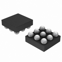
Package / Case
9-FlipChip
Operational Class
Class-D
Audio Amplifier Output Configuration
1-Channel Mono
Output Power (typ)
2.63x1@4OhmW
Audio Amplifier Function
Speaker
Total Harmonic Distortion
0.05@8Ohm@0.25W%
Single Supply Voltage (typ)
3/5V
Dual Supply Voltage (typ)
Not RequiredV
Power Supply Requirement
Single
Rail/rail I/o Type
No
Power Supply Rejection Ratio
65dB
Single Supply Voltage (min)
2.5V
Single Supply Voltage (max)
5.5V
Dual Supply Voltage (min)
Not RequiredV
Dual Supply Voltage (max)
Not RequiredV
Operating Temp Range
-40C to 85C
Operating Temperature Classification
Industrial
Mounting
Surface Mount
Pin Count
9
Lead Free Status / RoHS Status
Lead free / RoHS Compliant
Available stocks
Company
Part Number
Manufacturer
Quantity
Price
Company:

Part Number:
NCP2820AFCT2G
Manufacturer:
ON Semiconductor
Quantity:
1 300
Part Number:
NCP2820AFCT2G
Manufacturer:
ON/安森美
Quantity:
20 000


PIN DESCRIPTION
Differential
Differential
CSP
Negative
A1
A2
A3
B1
B2
B3
C1
C2
C3
Positive
Input
Input
Pin No.
UDFN8
3
7
8
2
6
7
4
1
5
R
R
i
i
Symbol
OUTM
OUTP
INM
GND
GND
INM
INP
SD
9-Pin Flip-Chip CSP
V
V
INP
A1
B1
VP
C1
p
p
INM
INP
(Top View)
GND
VP
SD
A2
C2
B2
Type
O
O
I
I
I
I
I
I
I
R
R
OUTM
GND
f
f
OUTP
B3
A3
C3
Positive Differential Input.
Analog Ground.
Negative BTL Output.
Analog Positive Supply. Range: 2.5 V – 5.5 V.
Power Analog Positive Supply. Range: 2.5 V – 5.5 V.
Analog Ground.
Negative Differential Input.
The device enters in Shutdown Mode when a low level is applied on this pin. An internal
300 kW resistor will force the device in shutdown mode if no signal is applied to this pin. It
also helps to save space and cost.
Positive BTL Output.
Figure 1. Typical Application
GENERATOR
PIN CONNECTIONS
NCP2820 Series
http://onsemi.com
RAMP
V
300 kW
ih
2
V
BATTERY
SD
p
V
Shutdown
il
Control
Cs
INM
INP
Processor
SD
VP
Data
Description
1
2
3
4
(Top View)
GND
UDFN8
CMOS
Output
Stage
OUTM
OUTP
8
7
6
5
OUTM
GND
VP
OUTP
Related parts for NCP2820AFCT2G
Image
Part Number
Description
Manufacturer
Datasheet
Request
R

Part Number:
Description:
2.65W Filterless Class-D Audio Power Amplifier
Manufacturer:
ON Semiconductor
Datasheet:
Part Number:
Description:
ON Semiconductor [VOLTAGE REGULATOR]
Manufacturer:
ON Semiconductor
Datasheet:
Part Number:
Description:
357-036-542-201 CARDEDGE 36POS DL .156 BLK LOPRO
Manufacturer:
ON Semiconductor
Datasheet:
Part Number:
Description:
357-036-542-201 CARDEDGE 36POS DL .156 BLK LOPRO
Manufacturer:
ON Semiconductor
Datasheet:
Part Number:
Description:
357-036-542-201 CARDEDGE 36POS DL .156 BLK LOPRO
Manufacturer:
ON Semiconductor
Datasheet:
Part Number:
Description:
357-036-542-201 CARDEDGE 36POS DL .156 BLK LOPRO
Manufacturer:
ON Semiconductor
Datasheet:
Part Number:
Description:
357-036-542-201 CARDEDGE 36POS DL .156 BLK LOPRO
Manufacturer:
ON Semiconductor
Datasheet:
Part Number:
Description:
357-036-542-201 CARDEDGE 36POS DL .156 BLK LOPRO
Manufacturer:
ON Semiconductor
Datasheet:
Part Number:
Description:
357-036-542-201 CARDEDGE 36POS DL .156 BLK LOPRO
Manufacturer:
ON Semiconductor
Datasheet:
Part Number:
Description:
357-036-542-201 CARDEDGE 36POS DL .156 BLK LOPRO
Manufacturer:
ON Semiconductor
Datasheet:
Part Number:
Description:
357-036-542-201 CARDEDGE 36POS DL .156 BLK LOPRO
Manufacturer:
ON Semiconductor
Datasheet:
Part Number:
Description:
357-036-542-201 CARDEDGE 36POS DL .156 BLK LOPRO
Manufacturer:
ON Semiconductor
Datasheet:
Part Number:
Description:
Manufacturer:
ON Semiconductor
Datasheet:
Part Number:
Description:
Manufacturer:
ON Semiconductor
Datasheet: