TDA8946AJ/N2,112 NXP Semiconductors, TDA8946AJ/N2,112 Datasheet - Page 20
TDA8946AJ/N2,112
Manufacturer Part Number
TDA8946AJ/N2,112
Description
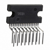
IC AMP AUDIO PWR 15W STER 17SIL
Manufacturer
NXP Semiconductors
Type
Class ABr
Datasheet
1.TDA8946AJN2112.pdf
(20 pages)
Specifications of TDA8946AJ/N2,112
Output Type
2-Channel (Stereo)
Package / Case
17-SIL (Bent and Staggered Leads)
Max Output Power X Channels @ Load
15W x 2 @ 8 Ohm
Voltage - Supply
4.5 V ~ 18 V
Features
Depop, Mute, Short-Circuit and Thermal Protection, Standby
Mounting Type
Through Hole
Product
Class-AB
Output Power
15 W
Available Set Gain
30 dB
Thd Plus Noise
0.07 %
Operating Supply Voltage
18 V
Maximum Power Dissipation
28000 mW
Maximum Operating Temperature
+ 85 C
Mounting Style
SMD/SMT
Audio Load Resistance
8 Ohms
Input Signal Type
Differential
Minimum Operating Temperature
- 40 C
Output Signal Type
Differential
Supply Type
Single
Supply Voltage (max)
18 V
Supply Voltage (min)
4.5 V
Lead Free Status / RoHS Status
Lead free / RoHS Compliant
Other names
568-3456-5
935270283112
TDA8946AJU
935270283112
TDA8946AJU


Philips Semiconductors
Contents
1
2
3
4
5
6
7
7.1
7.2
8
8.1
8.2
8.2.1
8.2.2
8.3
8.3.1
8.4
8.5
8.6
8.6.1
8.6.2
9
10
11
12
13
14
14.1
14.1.1
14.1.2
14.2
15
15.1
15.1.1
16
17
17.1
17.2
17.3
17.4
18
19
20
21
© Koninklijke Philips Electronics N.V. 2002.
Printed in The Netherlands
All rights are reserved. Reproduction in whole or in part is prohibited without the prior
written consent of the copyright owner.
The information presented in this document does not form part of any quotation or
contract, is believed to be accurate and reliable and may be changed without notice. No
liability will be accepted by the publisher for any consequence of its use. Publication
thereof does not convey nor imply any license under patent- or other industrial or
intellectual property rights.
Date of release: 01 March 2002
General description . . . . . . . . . . . . . . . . . . . . . . 1
Features . . . . . . . . . . . . . . . . . . . . . . . . . . . . . . . 1
Applications . . . . . . . . . . . . . . . . . . . . . . . . . . . . 1
Quick reference data . . . . . . . . . . . . . . . . . . . . . 1
Ordering information . . . . . . . . . . . . . . . . . . . . . 2
Block diagram . . . . . . . . . . . . . . . . . . . . . . . . . . 2
Pinning information . . . . . . . . . . . . . . . . . . . . . . 3
Functional description . . . . . . . . . . . . . . . . . . . 4
Limiting values. . . . . . . . . . . . . . . . . . . . . . . . . . 7
Thermal characteristics. . . . . . . . . . . . . . . . . . . 7
Static characteristics. . . . . . . . . . . . . . . . . . . . . 8
Dynamic characteristics . . . . . . . . . . . . . . . . . . 9
Internal circuitry. . . . . . . . . . . . . . . . . . . . . . . . 12
Application information. . . . . . . . . . . . . . . . . . 14
Test information . . . . . . . . . . . . . . . . . . . . . . . . 16
Package outline . . . . . . . . . . . . . . . . . . . . . . . . 17
Soldering . . . . . . . . . . . . . . . . . . . . . . . . . . . . . 18
Revision history . . . . . . . . . . . . . . . . . . . . . . . . 18
Data sheet status . . . . . . . . . . . . . . . . . . . . . . . 19
Definitions . . . . . . . . . . . . . . . . . . . . . . . . . . . . 19
Disclaimers . . . . . . . . . . . . . . . . . . . . . . . . . . . . 19
Pinning . . . . . . . . . . . . . . . . . . . . . . . . . . . . . . . 3
Pin description . . . . . . . . . . . . . . . . . . . . . . . . . 3
Input configuration . . . . . . . . . . . . . . . . . . . . . . 4
Power amplifier . . . . . . . . . . . . . . . . . . . . . . . . . 5
Output power measurement . . . . . . . . . . . . . . . 5
Headroom . . . . . . . . . . . . . . . . . . . . . . . . . . . . . 5
Mode selection . . . . . . . . . . . . . . . . . . . . . . . . . 6
Switch-on and switch off . . . . . . . . . . . . . . . . . . 6
DC gain control . . . . . . . . . . . . . . . . . . . . . . . . . 6
Supply Voltage Ripple Rejection (SVRR) . . . . . 6
Built-in protection circuits . . . . . . . . . . . . . . . . . 7
Short-circuit protection . . . . . . . . . . . . . . . . . . . 7
Thermal shutdown protection . . . . . . . . . . . . . . 7
Printed-circuit board . . . . . . . . . . . . . . . . . . . . 14
Layout and grounding . . . . . . . . . . . . . . . . . . . 14
Power supply decoupling . . . . . . . . . . . . . . . . 15
Thermal behaviour and heatsink calculation . 15
Quality information . . . . . . . . . . . . . . . . . . . . . 16
Test conditions . . . . . . . . . . . . . . . . . . . . . . . . 16
Introduction to soldering through-hole
Soldering by dipping or by solder wave . . . . . 18
Manual soldering . . . . . . . . . . . . . . . . . . . . . . 18
Package related soldering information . . . . . . 18
mount packages . . . . . . . . . . . . . . . . . . . . . . 18
Document order number: 9397 750 09434
2 x 15 W BTL audio amplifier with DC gain control
TDA8946AJ
Related parts for TDA8946AJ/N2,112
Image
Part Number
Description
Manufacturer
Datasheet
Request
R

Part Number:
Description:
Tda8946aj 2 X 15 W Btl Audio Amplifier With Dc Gain Control
Manufacturer:
NXP Semiconductors
Datasheet:

Part Number:
Description:
2 x 15 W stereo Bridge Tied Load BTL audio amplifier
Manufacturer:
Philips Semiconductors
Datasheet:
Part Number:
Description:
NXP Semiconductors designed the LPC2420/2460 microcontroller around a 16-bit/32-bitARM7TDMI-S CPU core with real-time debug interfaces that include both JTAG andembedded trace
Manufacturer:
NXP Semiconductors
Datasheet:

Part Number:
Description:
NXP Semiconductors designed the LPC2458 microcontroller around a 16-bit/32-bitARM7TDMI-S CPU core with real-time debug interfaces that include both JTAG andembedded trace
Manufacturer:
NXP Semiconductors
Datasheet:
Part Number:
Description:
NXP Semiconductors designed the LPC2468 microcontroller around a 16-bit/32-bitARM7TDMI-S CPU core with real-time debug interfaces that include both JTAG andembedded trace
Manufacturer:
NXP Semiconductors
Datasheet:
Part Number:
Description:
NXP Semiconductors designed the LPC2470 microcontroller, powered by theARM7TDMI-S core, to be a highly integrated microcontroller for a wide range ofapplications that require advanced communications and high quality graphic displays
Manufacturer:
NXP Semiconductors
Datasheet:
Part Number:
Description:
NXP Semiconductors designed the LPC2478 microcontroller, powered by theARM7TDMI-S core, to be a highly integrated microcontroller for a wide range ofapplications that require advanced communications and high quality graphic displays
Manufacturer:
NXP Semiconductors
Datasheet:
Part Number:
Description:
The Philips Semiconductors XA (eXtended Architecture) family of 16-bit single-chip microcontrollers is powerful enough to easily handle the requirements of high performance embedded applications, yet inexpensive enough to compete in the market for hi
Manufacturer:
NXP Semiconductors
Datasheet:
Part Number:
Description:
The XA-S3 device is a member of Philips Semiconductors? XA(eXtended Architecture) family of high performance 16-bitsingle-chip microcontrollers
Manufacturer:
NXP Semiconductors
Datasheet:

Part Number:
Description:
The NXP BlueStreak LH75401/LH75411 family consists of two low-cost 16/32-bit System-on-Chip (SoC) devices
Manufacturer:
NXP Semiconductors
Datasheet:
Part Number:
Description:
The NXP LPC3130/3131 combine an 180 MHz ARM926EJ-S CPU core, high-speed USB2
Manufacturer:
NXP Semiconductors
Datasheet:
Part Number:
Description:
The NXP LPC3141 combine a 270 MHz ARM926EJ-S CPU core, High-speed USB 2
Manufacturer:
NXP Semiconductors
Part Number:
Description:
The NXP LPC3143 combine a 270 MHz ARM926EJ-S CPU core, High-speed USB 2
Manufacturer:
NXP Semiconductors

Part Number:
Description:
The NXP LPC3152 combines an 180 MHz ARM926EJ-S CPU core, High-speed USB 2
Manufacturer:
NXP Semiconductors