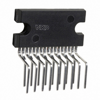
TDA8946AJ/N2,112 NXP Semiconductors, TDA8946AJ/N2,112 Datasheet - Page 9

TDA8946AJ/N2,112
Manufacturer Part Number
TDA8946AJ/N2,112
Description
IC AMP AUDIO PWR 15W STER 17SIL
Manufacturer
NXP Semiconductors
Type
Class ABr
Datasheet
1.TDA8946AJN2112.pdf
(20 pages)
Specifications of TDA8946AJ/N2,112
Output Type
2-Channel (Stereo)
Package / Case
17-SIL (Bent and Staggered Leads)
Max Output Power X Channels @ Load
15W x 2 @ 8 Ohm
Voltage - Supply
4.5 V ~ 18 V
Features
Depop, Mute, Short-Circuit and Thermal Protection, Standby
Mounting Type
Through Hole
Product
Class-AB
Output Power
15 W
Available Set Gain
30 dB
Thd Plus Noise
0.07 %
Operating Supply Voltage
18 V
Maximum Power Dissipation
28000 mW
Maximum Operating Temperature
+ 85 C
Mounting Style
SMD/SMT
Audio Load Resistance
8 Ohms
Input Signal Type
Differential
Minimum Operating Temperature
- 40 C
Output Signal Type
Differential
Supply Type
Single
Supply Voltage (max)
18 V
Supply Voltage (min)
4.5 V
Lead Free Status / RoHS Status
Lead free / RoHS Compliant
Other names
568-3456-5
935270283112
TDA8946AJU
935270283112
TDA8946AJU
Philips Semiconductors
12. Dynamic characteristics
Table 8:
V
unless otherwise specified.
[1]
[2]
[3]
9397 750 09434
Product data
Symbol
P
THD
G
G
V
Z
V
SVRR
V
CC
Fig 6. Voltage gain as function of control voltage.
o
i(rms)
i(dif)
n(o)
o(mute)
cs
v(max)
v(cr)
G
handbook, halfpage
v
= 18 V; T
The noise output voltage is measured at the output in a frequency range from 20 Hz to 20 kHz (unweighted), with a source impedance
R
Supply voltage ripple rejection is measured at the output, with a source impedance R
wave with a frequency f
Output voltage in mute mode is measured with V
noise.
source
V
(dB)
G v
CC
40
20
20
40
60
80
= 18 V
0
= 0
0
Dynamic characteristics
amb
Parameter
output power
total harmonic distortion
maximum voltage gain
gain control range
input voltage (RMS value)
differential input impedance
noise output voltage
supply voltage ripple rejection
output voltage
channel separation
channel unbalance
at the input.
= 25 C; R
1
ripple
L
= 8 ; f = 1 kHz; V
and an amplitude of 700 mV (RMS), which is applied to the positive supply rail.
2
3
V GC (V)
MGW613
GC
MODE
4
Rev. 01 — 01 March 2002
= 0 V and an input voltage of 1 V (RMS) in a bandwidth of 20 kHz, thus including
Conditions
THD = 10%
THD = 0.5%
P
0.5 < V
G
V
V
f
f
mute mode
R
G
ripple
ripple
o
GC
GC
source
v
v
= 0 V; G
= 1 W
= 0 dB; THD <1%
= 0 dB; V
= 4.0 V
= 1.0 V
= 1 kHz
= 100 Hz to 20 kHz
GC
= 0
< 4.0 V
v
= 30 dB; V
GC
Fig 7. Output voltage as function of mode voltage.
handbook, halfpage
2 x 15 W BTL audio amplifier with DC gain control
= 1.8 V
V
(V)
V o
i
10
10
10
10
10
= 30 mV; V
10
1
1
2
3
4
5
0
GC
= 4.0 V; measured in test circuit
source
CC
4
[1]
[1]
[2]
[2]
[3]
= 18 V
= 0
Min
13
-
-
29
-
1.0
50
-
-
-
-
-
50
-
8
at the input. The ripple voltage is a sine
© Koninklijke Philips Electronics N.V. 2002. All rights reserved.
Typ
15
11.5
0.07
30
80
-
65
120
30
55
55
30
75
-
12
TDA8946AJ
V MODE (V)
16
Max
-
-
0.5
31
-
-
-
170
-
-
-
50
-
1
MGW614
Figure
20
15;
Unit
W
W
%
dB
dB
V
k
dB
dB
dB
dB
9 of 20
V
V
V


