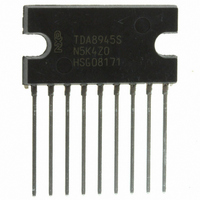
TDA8945S/N1,112 NXP Semiconductors, TDA8945S/N1,112 Datasheet - Page 4

TDA8945S/N1,112
Manufacturer Part Number
TDA8945S/N1,112
Description
IC AMP AUDIO PWR 15W MONO 9SIL
Manufacturer
NXP Semiconductors
Type
Class ABr
Datasheet
1.TDA8945SN1112.pdf
(21 pages)
Specifications of TDA8945S/N1,112
Output Type
1-Channel (Mono)
Package / Case
9-SIL (Straight Leads)
Max Output Power X Channels @ Load
15W x 1 @ 8 Ohm
Voltage - Supply
6 V ~ 25 V
Features
Depop, Mute, Short-Circuit and Thermal Protection, Standby
Mounting Type
Through Hole
Product
Class-AB
Output Power
15 W
Available Set Gain
32 dB
Thd Plus Noise
0.03 %
Operating Supply Voltage
18 V
Maximum Power Dissipation
14000 mW
Maximum Operating Temperature
+ 70 C
Mounting Style
Through Hole
Audio Load Resistance
8 Ohms
Input Signal Type
Differential
Minimum Operating Temperature
- 40 C
Output Signal Type
Differential
Supply Type
Single
Supply Voltage (max)
25 V
Supply Voltage (min)
6 V
Operational Class
Class-AB
Audio Amplifier Output Configuration
1-Channel Mono
Output Power (typ)
15x1@8OhmW
Audio Amplifier Function
Speaker
Total Harmonic Distortion
0.03@8Ohm@1W%
Single Supply Voltage (typ)
18V
Dual Supply Voltage (typ)
Not RequiredV
Power Supply Requirement
Single
Power Dissipation
14W
Rail/rail I/o Type
No
Single Supply Voltage (min)
6V
Single Supply Voltage (max)
25V
Dual Supply Voltage (min)
Not RequiredV
Dual Supply Voltage (max)
Not RequiredV
Operating Temp Range
-40C to 70C
Operating Temperature Classification
Commercial
Mounting
Through Hole
Pin Count
9
Lead Free Status / RoHS Status
Lead free / RoHS Compliant
Lead Free Status / RoHS Status
Lead free / RoHS Compliant, Lead free / RoHS Compliant
Other names
568-3509-5
935262856112
TDA8945SU
935262856112
TDA8945SU
Available stocks
Company
Part Number
Manufacturer
Quantity
Price
Company:
Part Number:
TDA8945S/N1,112
Manufacturer:
ICSI
Quantity:
4 379
Philips Semiconductors
9397 750 06866
Product specification
8.2.1 Output power measurement
8.1 Input configuration
8.2 Power amplifier
The TDA8945S inputs can be driven symmetrical (floating) as well as asymmetrical.
In the asymmetrical mode one input pin is connected via a capacitor to the signal
ground which should be as close as possible to the SVR (electrolytic) capacitor
ground. Note that the DC level of the input pins is half of the supply voltage V
coupling capacitors for both pins are necessary.
The input cut-off frequency is:
For R
As shown in
necessary;
minimized. This results in a good low frequency response and good switch-on
behaviour.
Remark: To prevent HF oscillations do not leave the inputs open, connect a capacitor
of at least 1.5 nF across the input pins close to the device.
The power amplifier is a Bridge Tied Load (BTL) amplifier with an all-NPN output
stage, capable of delivering a peak output current of 2 A.
The BTL principle offers the following advantages:
The output power as a function of the supply voltage is measured on the output pins
at THD = 10%; see
supply voltage of 18 V and the maximum available output current: 2 A repetitive peak
current.
f
f
•
•
•
•
i cut off
i cut off
Lower peak value of the supply current
The ripple frequency on the supply voltage is twice the signal frequency
No expensive DC-blocking capacitor
Good low frequency performance.
i
–
–
= 45 k and C
=
=
so the switch-on delay during charging of the input capacitors, can be
Equation 1
---------------------------- -
2
---------------------------------------------------------------- -
2
R
45 10
1
i
Rev. 02 — 7 April 2000
Figure
i
C
= 220 nF:
i
3
and 2, large capacitor values for the inputs are not
1
8. The maximum output power is limited by the maximum
220 10
9 –
=
16 Hz
15 W mono BTL audio amplifier
© Philips Electronics N.V. 2000. All rights reserved.
TDA8945S
CC
, so
4 of 21
(1)
(2)


