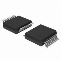
TDA9889TS/V1,518 NXP Semiconductors, TDA9889TS/V1,518 Datasheet - Page 6

TDA9889TS/V1,518
Manufacturer Part Number
TDA9889TS/V1,518
Description
IC AGC AMPLIFIER 16SSOP
Manufacturer
NXP Semiconductors
Datasheet
1.TDA9889TSV1518.pdf
(22 pages)
Specifications of TDA9889TS/V1,518
Applications
Automatic Gain Control (AGC)
Number Of Circuits
1
Current - Supply
55mA
Voltage - Supply, Single/dual (±)
4.5 V ~ 5.5 V
Mounting Type
Surface Mount
Package / Case
16-SSOP (0.200", 5.30mm Width)
Lead Free Status / RoHS Status
Lead free / RoHS Compliant
Other names
935269701518
TDA9889TSDB-T
TDA9889TSDB-T
TDA9889TSDB-T
TDA9889TSDB-T
Philips Semiconductors
Reference generation
The 4 MHz crystal is the reference for the downconversion
synthesizer and the filter synthesizer.
The downconverted DVB frequency and the frequency
adjustment of the integrated filters are dependent on the
precision of the reference signal at pin REF. An operation
as crystal oscillator is possible as well as connecting this
input via a serial capacitor to another low-ohmic reference
frequency source.
The integrated divider-by-8 generates the internally
needed 500 kHz reference frequency for the DVB
synthesizer and the reference filter.
Synthesizer for downconversion
The PLL synthesizer for downconversion consists of a
Voltage Controlled Oscillator (VCO), a divider with a
standard dependent divider factor, a frequency phase
detector (constructed as a digital 3-state comparator) and
a charge pump.
The VCO operates as an integrated low radiation
relaxation oscillator at double the conversion frequency.
For downconversion the VCO frequency is divided-by-2 to
provide two differential square wave signals with exactly
90 degrees phase difference, independent of the VCO
frequency.
The frequency phase detector compares the down-divided
oscillator signal with the 500 kHz reference frequency
signal and controls, via the charge pump, the control
voltage at the external loop filter connected to pin LFS,
which is required to tune the VCO exactly to the wanted
frequency.
The divider, the frequency phase detector and the
reference frequency divider are constructed in a low
radiation technique to optimize the synthesizer spurious
suppression in the downconverted output signal.
Downconversion and complex filtering
The gain controlled IF signal from the IF amplifier is fed to
two identical linear mixers, operating in the ‘in phase’ and
‘quadrature’ mode in accordance to the 0 and 90 degree
VCO signal from the synthesizer. With this, the
downconverted DVB low IF signal is available as an
I and Q signal in the frequency band from 1 to 9 MHz.
These signals are fed to the complex filter section. As a
result of adding both signals, the unwanted mirror signal
will be attenuated (approximately 34 dB). The unwanted
frequency components below 1 MHz are attenuated in a
high-pass filter. This signal is then fed through a
group-delay equalizer circuit.
2004 Nov 02
DVB selective AGC amplifier
6
Tracking low-pass filter with reference control
The low-pass filter is controlled by a reference signal
[generated by a frequency synthesizer and can be
switched by the standard selection (S0 and S1)].
The tracking low-pass filter is designed as a
Tschebyscheff filter to guarantee sufficient suppression for
the neighbouring picture carrier. An all-pass filter corrects
the characteristic to obtain a flat (equivalent ripple) group
delay behaviour.
Low IF differential output stage
The output amplifier consists of two identical differential
operational amplifiers with a high common mode (DC)
rejection ratio, to provide a constant DC voltage at the
output stage. The amplified Low IF (LIF) signal is available
as a differential signal with an amplitude of 2 V (p-p) and
DC level of 2 V (typ.) between the output terminals of both
amplifiers.
Logic control
The logic control provides an easy selection of the most
common standards for Europe, USA and Japan with the
two switches S0 and S1 (frequency selection different for
TDA9888TS and TDA9889TS) and controls all internal
standard dependent stages.
The five available tuner AGC modes can be set via the
3-state input pin S2 and R
Internal voltage stabilizer
The band gap circuit generates a voltage of approximately
2.4 V, independent of the supply voltage and the
temperature. A voltage regulator circuit, controlled by this
voltage, produces a constant voltage of 3.55 V which is
used as an internal reference voltage.
TDA9888TS; TDA9889TS
TOP
connection (at pin TADJ).
Product specification


