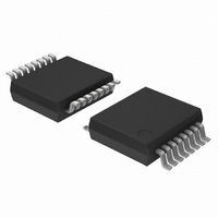
TDA9889TS/V1,518 NXP Semiconductors, TDA9889TS/V1,518 Datasheet - Page 8

TDA9889TS/V1,518
Manufacturer Part Number
TDA9889TS/V1,518
Description
IC AGC AMPLIFIER 16SSOP
Manufacturer
NXP Semiconductors
Datasheet
1.TDA9889TSV1518.pdf
(22 pages)
Specifications of TDA9889TS/V1,518
Applications
Automatic Gain Control (AGC)
Number Of Circuits
1
Current - Supply
55mA
Voltage - Supply, Single/dual (±)
4.5 V ~ 5.5 V
Mounting Type
Surface Mount
Package / Case
16-SSOP (0.200", 5.30mm Width)
Lead Free Status / RoHS Status
Lead free / RoHS Compliant
Other names
935269701518
TDA9889TSDB-T
TDA9889TSDB-T
TDA9889TSDB-T
TDA9889TSDB-T
Philips Semiconductors
CHARACTERISTICS
V
V
1 : 1; gain controlled amplifier adjusted to low IF differential output of 2 V (p-p); measurements taken in test circuit of
Fig.11 with external 4 MHz reference signal of 140 mV (RMS); unless otherwise specified.
2004 Nov 02
Supply; pin V
V
I
P
IF amplifier; pins IF1 and IF2; differential
G
G
G
B
B
R
C
V
Low IF output signal; pins LIF1 and LIF2; differential; see Fig.8
V
V
V
R
V
I
I
I
Z
t
P
bias(int)
o(source)(max)
o(sink)(max)
d(g)(LIF)
P
i(IF)(rms)
SYMBOL
L(diff)
P
tot
IF( 3dB)(ll)
IF( 3dB)(ul)
I
o(LIF)(p-p)
clip(u)
clip(l)
O
LIF
N 1
27MHz
i(dif)
i(dif)
o(diff)
DVB selective AGC amplifier
IF(max)
IF(min)
IF(cr)
= 5 V; T
= 10 mV frequency f
amb
supply voltage
supply current
total power dissipation
maximum conversion gain
minimum conversion gain
IF gain control range
lower limit 3 dB IF bandwidth
upper limit 3 dB IF bandwidth note 2
differential input resistance
differential input capacitance
DC input voltage
typical low IF operating output
voltage (peak-to-peak value)
upper clipping voltage level
(single-ended)
lower clipping voltage level
(single-ended)
output resistance (differential)
DC output voltage
internal DC bias current for
emitter-follower (single-ended)
maximum AC and DC output
source current (single-ended)
maximum AC and DC output
sink current (single-ended)
differential load impedance
low IF band amplitude
characteristic
low IF band group delay ripple
low-pass filter attenuation
low-pass filter attenuation
= 25 C; 8 MHz system; see Tables 1 or 2, CW test input signal is used for specification;
P
PARAMETER
IF
= 36 MHz for low IF output of 5 MHz; IF input from 50
note 1
output peak-to-peak level to
input RMS level ratio
see Fig.3
note 2
note 2
note 2
note 2
note 3
note 2
0 dB at middle of band
(standard independent)
from 1 MHz to 2 MHz
from 2 MHz to end of band
6 MHz band; at 11.75 MHz
7 MHz band; at 13.75 MHz
8 MHz band; at 15.75 MHz
any band; at 27 MHz
CONDITIONS
8
TDA9888TS; TDA9889TS
4.5
46
85
60
2.9
0.8
2.5
0.6
1.7
15
15
15
40
0.9
MIN.
via broadband transformer
5
55
275
90
20
70
15
80
2
3
1.9
2
2
1
50
TYP.
Product specification
5.5
64
352
23
0.6
150
+0.9
150
100
MAX.
V
mA
mW
dB
dB
dB
MHz
MHz
k
pF
V
V
V
V
V
mA
mA
mA
k
dB
ns
ns
dB
dB
dB
dB
UNIT


