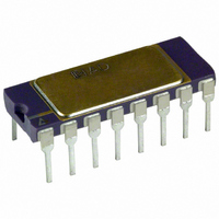
AD539JD Analog Devices Inc, AD539JD Datasheet - Page 11

AD539JD
Manufacturer Part Number
AD539JD
Description
IC MULT/DIV DUAL CH LIN 16-CDIP
Manufacturer
Analog Devices Inc
Specifications of AD539JD
Rohs Status
RoHS non-compliant
Function
Analog Multiplier/Divider
Number Of Bits/stages
2
Package / Case
16-CDIP (0.300", 7.62mm)
Number Of Elements
2
Output Type
Single
Power Supply Requirement
Dual
Single Supply Voltage (typ)
Not RequiredV
Single Supply Voltage (min)
Not RequiredV
Single Supply Voltage (max)
Not RequiredV
Dual Supply Voltage (typ)
±5/±9/±12V
Dual Supply Voltage (min)
±4.5V
Dual Supply Voltage (max)
±15V
Operating Temperature Classification
Commercial
Mounting
Through Hole
Pin Count
16
Package Type
SBCDIP
Lead Free Status / RoHS Status
Not Compliant
Available stocks
Company
Part Number
Manufacturer
Quantity
Price
Part Number:
AD539JD
Manufacturer:
ADI/亚德诺
Quantity:
20 000
The power supplies to the AD539 can be as low as ±4.5 V and as
high as ±16.5 V. The maximum allowable range of the signal
inputs, V
value is 2.5 V above −V
inputs of ±4.2 V the supplies should be nominally +5 V and
−7.5 V. Although there is no performance advantage in raising
supplies above these values, it may often be convenient to use
the same supplies as for the op amps. The AD539 can tolerate
the excess voltage with only a slight effect on dc accuracy but
dissipation at ±16.5 V can be as high as 535 mW, and some
form of heat sink is essential in the interests of reliability.
TRANSFER FUNCTION
In using any analog multiplier or divider, careful attention must
be paid to the matter of scaling, particularly in computational
applications. To be dimensionally consistent, a scaling voltage
must appear in the transfer function, which, for each channel
of the AD539 in the standard multiplier configuration (see
Figure 20), is
where the V
voltage, V
In this case, V
acceptable in the interest of simplification to use the less rigorous
expression
where it is understood that all signals must be expressed in volts,
that is, they are rendered dimensionless by division by 1 V.
The accuracy specifications for V
two feedback resistors supplied with each channel, because
these are very closely matched, or they can be used in parallel to
halve the gain (double the effective scaling voltage), when
When an external load resistor, R
longer exact because the internal thin film resistors, although
trimmed to high ratiometric accuracy, have an absolute
tolerance of 20%. However, the nominal transfer function is
where the effective scaling voltage, V
each channel using the formula
where R
100 Ω, V
case where both channels are used in parallel. The AD539 can
V
V
V
V
V
W
W
W
W
U
’ = V
L
= −V
= −V
= −V
= −V
U
Y
is expressed in kilohms. For example, when R
U
’ = 67.5 V. Table 5 provides more detailed data for the
, is approximately 0.5 V above +V
, are expressed in a consistent unit, usually volts.
X
U
X
and V
X
X
X
(5R
U
V
V
V
V
is fixed by the design to be 1 V and it is often
Y
Y
Y
Y
/V
/2
/V
L
+ 6.25)/R
U
Y
U
’
inputs, the V
S
. To accommodate the peak specified
L
L
U
W
, is used, the scaling is no
allow the use of either of the
output, and the scaling
U
’ , can be calculated for
S
; the minimum
L
=
Rev. B | Page 11 of 20
also be used with no external load (CHAN2 OUTPUT, Pin 11,
or CHAN1 OUTPUT, Pin 14, open circuit), when VU’ is
precisely 5 V.
DUAL SIGNAL CHANNELS
The signal voltage inputs, V
(FS) values of ±2 V with a peak range to ±4.2 V (using a negative
supply of 7.5 V or greater). For video applications where
differential phase is critical, a reduced input range of ±1 V is
recommended, resulting in a phase variation of typically ±0.2°
at 3.579 MHz for full gain. The input impedance is typically
400 kΩ shunted by 3 pF. Signal channel distortion is typically
well under 0.1% at 10 kHz and can be reduced to 0.01% by using
the channels differentially.
COMMON CONTROL CHANNEL
The control channel accepts positive inputs, V
FS, ±3.3 V peak. The input resistance is 500 Ω. An external,
grounded capacitor determines the small-signal bandwidth and
recovery time of the control amplifier; the minimum value of
3 nF allows a bandwidth at midgain of about 5 MHz. Larger
compensation capacitors slow the control channel but improve
the high frequency performance of the signal channels.
FLEXIBLE SCALING
Using either one or two external op amps in conjunction with
the on-chip 6 kΩ scaling resistors (see Figure 19), the output
currents (nominally ±1 mA FS, ±2.25 mA peak) can be
converted to voltages with accurate transfer functions of V
−V
inputs and V
ing full-scale outputs of ±3 V, ±6 V, and ±12 V. Alternatively,
low impedance grounded loads can be used to achieve the full
signal bandwidth of 60 MHz, in which mode the scaling is less
accurate.
Figure 19. Block Diagram Showing Scaling Resistors and External Op Amps
X
V
Y
/2, V
V
V
V
Z1
Z2
Y1
Y2
X
W
W
= −V
output are expressed in volts), with correspond-
MULTIPLY
MULTIPLY
CHAN1
CHAN2
X
V
Y
, or V
Y1
W
–
–
and V
= −2V
EXTRNAL
OP AMPS
Y2
X
, have nominal full-scale
V
Y
(where the V
W1
V
V
W2
W1
W2
= –V
= –V
X
, from 0 V to 3 V
X
X
V
V
Y1
Y2
X
AD539
and V
W
=
Y


