AD539JD Analog Devices Inc, AD539JD Datasheet - Page 2
AD539JD
Manufacturer Part Number
AD539JD
Description
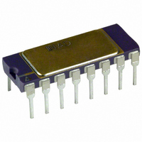
IC MULT/DIV DUAL CH LIN 16-CDIP
Manufacturer
Analog Devices Inc
Specifications of AD539JD
Rohs Status
RoHS non-compliant
Function
Analog Multiplier/Divider
Number Of Bits/stages
2
Package / Case
16-CDIP (0.300", 7.62mm)
Number Of Elements
2
Output Type
Single
Power Supply Requirement
Dual
Single Supply Voltage (typ)
Not RequiredV
Single Supply Voltage (min)
Not RequiredV
Single Supply Voltage (max)
Not RequiredV
Dual Supply Voltage (typ)
±5/±9/±12V
Dual Supply Voltage (min)
±4.5V
Dual Supply Voltage (max)
±15V
Operating Temperature Classification
Commercial
Mounting
Through Hole
Pin Count
16
Package Type
SBCDIP
Lead Free Status / RoHS Status
Not Compliant
Available stocks
Company
Part Number
Manufacturer
Quantity
Price

Part Number:
AD539JD
Manufacturer:
ADI/亚德诺
Quantity:
20 000


TABLE OF CONTENTS
Features .............................................................................................. 1
Applications....................................................................................... 1
Functional Block Diagram .............................................................. 1
General Description ......................................................................... 1
Revision History ............................................................................... 2
Specifications..................................................................................... 3
Pin Configurations and Function Descriptions ........................... 5
Typical Performance Characteristics ............................................. 7
Theory of Operation ...................................................................... 10
REVISION HISTORY
4/11—Rev. A to Rev. B
Updated Format..................................................................Universal
Changed Pin Configuration to Functional Block Diagram........ 1
Changes to General Description Section ...................................... 1
Added Pin Configurations and Function Descriptions
Section................................................................................................ 5
Added Table 2; Renumbered Sequentially .................................... 5
Added Table 3.................................................................................... 6
Added Typical Performance Characteristics Section .................. 7
Added Figure 6 and Figure 9; Renumbered Sequentially ........... 7
Changes to Figure 18...................................................................... 10
AD539
Circuit Description..................................................................... 10
General Recommendations....................................................... 10
Rev. B | Page 2 of 20
Applications Information .............................................................. 12
Outline Dimensions ....................................................................... 17
Moved Dual Signal Channels Section, Common Control
Channel Section, and Flexible Scaling Section........................... 11
Changes to Figure 20...................................................................... 12
Changes to Table 4, Figure 21, and Table 5 ................................. 13
Changes to Figure 22 and Figure 23............................................. 14
Changes to Figure 24...................................................................... 15
Changes to Figure 25...................................................................... 16
Updated Outline Dimensions....................................................... 17
Changes to Ordering Guide .......................................................... 18
12/91—Rev. 0 to Rev. A
Transfer Function....................................................................... 11
Dual Signal Channels................................................................. 11
Common Control Channel....................................................... 11
Flexible Scaling ........................................................................... 11
Basic Multiplier Connections ................................................... 12
A 50 MHz Voltage-Controlled Amplifier ............................... 15
Basic Divider Connections ....................................................... 16
Ordering Guide .......................................................................... 18
Related parts for AD539JD
Image
Part Number
Description
Manufacturer
Datasheet
Request
R

Part Number:
Description:
±1.7g Dual-Axis IMEMS Accelerometer Evaluation Board
Manufacturer:
Analog Devices Inc
Datasheet:

Part Number:
Description:
Inertial Sensor Evaluation System
Manufacturer:
Analog Devices Inc
Datasheet:
Part Number:
Description:
Manufacturer:
Analog Devices Inc
Datasheet:
Part Number:
Description:
Manufacturer:
Analog Devices Inc
Datasheet:
Part Number:
Description:
Manufacturer:
Analog Devices Inc
Datasheet:
Part Number:
Description:
Manufacturer:
Analog Devices Inc
Datasheet:
Part Number:
Description:
Manufacturer:
Analog Devices Inc
Datasheet:
Part Number:
Description:
Manufacturer:
Analog Devices Inc
Datasheet:
Part Number:
Description:
Manufacturer:
Analog Devices Inc
Datasheet:
Part Number:
Description:
Manufacturer:
Analog Devices Inc
Datasheet:
Part Number:
Description:
Manufacturer:
Analog Devices Inc
Datasheet:
Part Number:
Description:
Manufacturer:
Analog Devices Inc
Datasheet:
Part Number:
Description:
Manufacturer:
Analog Devices Inc
Datasheet: