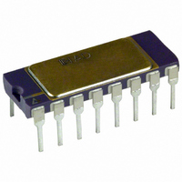
AD539JD Analog Devices Inc, AD539JD Datasheet - Page 14

AD539JD
Manufacturer Part Number
AD539JD
Description
IC MULT/DIV DUAL CH LIN 16-CDIP
Manufacturer
Analog Devices Inc
Specifications of AD539JD
Rohs Status
RoHS non-compliant
Function
Analog Multiplier/Divider
Number Of Bits/stages
2
Package / Case
16-CDIP (0.300", 7.62mm)
Number Of Elements
2
Output Type
Single
Power Supply Requirement
Dual
Single Supply Voltage (typ)
Not RequiredV
Single Supply Voltage (min)
Not RequiredV
Single Supply Voltage (max)
Not RequiredV
Dual Supply Voltage (typ)
±5/±9/±12V
Dual Supply Voltage (min)
±4.5V
Dual Supply Voltage (max)
±15V
Operating Temperature Classification
Commercial
Mounting
Through Hole
Pin Count
16
Package Type
SBCDIP
Lead Free Status / RoHS Status
Not Compliant
Available stocks
Company
Part Number
Manufacturer
Quantity
Price
Part Number:
AD539JD
Manufacturer:
ADI/亚德诺
Quantity:
20 000
Differential Configurations
When only one signal channel must be handled, it is often
advantageous to use the channels differentially. By subtracting
the Channel 1 and Channel 2 outputs, any residual transient
control feedthrough is virtually eliminated. Figure 22 shows a
minimal configuration where it is assumed that the host system
uses differential signals and a 50 Ω environment throughout.
This figure also shows a recommended control feedforward
network to improve large-signal response time. The control
feedthrough glitch is shown in Figure 12, where the input was
applied to Channel 1 and only the output of Channel 1 was
displayed on the oscilloscope. The improvement obtained when
CH1 and CH2 outputs are viewed differentially is clear in
Figure 13. The envelope rise time is of the order of 40 ns.
CONTROL
Lower distortion results when Channel 1 and Channel 2 are
driven by complementary inputs and the outputs are utilized
differentially, using a circuit such as the one shown in Figure 23.
Resistors R1 and R2 minimize a secondary distortion mechanism
AD539
CHAN1
CHAN2
INPUT
INPUT
INPUT
(V
S
)
56Ω
51Ω
51Ω
Figure 22. High Speed Differential Configuration
5nF
(16-Lead SBDIP and PDIP Shown)
0.1µF
0.1µF
100Ω
150pF
+5V
–5V
1
2
3
4
5
6
7
8
V
HF COMP
V
+V
–V
V
INPUT
COMMON
OUTPUT
COMMON
X
Y1
Y2
S
S
AD539
COMMON
OUTPUT
OUTPUT
BASE
CHAN1
CHAN2
W2
W1
Z1
Z2
16
15
14
13
12
10
11
9
CHAN1
OUTPUT
CHAN2
OUTPUT
Rev. B | Page 14 of 20
caused by a collector modulation effect in the controlled cascode
stages (see the Theory of Operation section) by keeping the
voltage swing at the outputs to an acceptable level and should
have a value in the range of 100 Ω to 1000 Ω. Figure 14 shows
the improvement in distortion over the standard configuration
(compare with Figure 5). Note that the Z nodes (Pin 10 and
Pin 15) are returned to the control input; this prevents the early
onset of output transistor saturation.
V
V
Even lower distortion (0.01%, or −80 dB) has been measured
using two output op amps in a configuration similar to that
shown in Figure 20 connected as virtual ground current summers
(to prevent the modulation effect). Note that to generate the
difference output it is merely necessary to connect the output of
the Channel 1 op amp to the Z node of Channel 2. In this way,
the net input to the Channel 2 op amp is the difference signal,
and the low distortion resultant appears as its output.
V
Y1
Y2
X
C
C
= 3nF
+V
–V
S
S
Figure 23. Low Distortion Differential Configuration
1
2
3
4
5
6
7
8
V
HF COMP
V
+V
–V
V
INPUT
COMMON
OUTPUT
COMMON
X
Y1
Y2
S
S
(16-Lead SBDIP and PDIP Shown)
AD539
COMMON
OUTPUT
OUTPUT
BASE
CHAN1
CHAN2
W1
W2
Z2
Z1
16
15
14
13
12
11
10
9
R1
R2
V
W
= V
X
(V
Y2
– V
Y1
)


