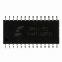
CS8427-CSZ Cirrus Logic Inc, CS8427-CSZ Datasheet - Page 52

CS8427-CSZ
Manufacturer Part Number
CS8427-CSZ
Description
IC TXRX DGTL AUDIO 96KHZ 28SOIC
Manufacturer
Cirrus Logic Inc
Type
Digital Audio Interface Transceiver (DIX)r
Datasheet
1.CS8427-DZZ.pdf
(60 pages)
Specifications of CS8427-CSZ
Applications
Automotive Audio
Mounting Type
Surface Mount
Package / Case
28-SOIC
Audio Control Type
Digital
Control Interface
I2C, Serial
Control / Process Application
AV & DVD Receivers, CD-R, Digital Mixing Consoles
Supply Voltage Range
2.85V To 5.5V
Lead Free Status / RoHS Status
Lead free / RoHS Compliant
For Use With
598-1783 - EVALUATION BOARD FOR CS8427
Lead Free Status / RoHS Status
Lead free / RoHS Compliant, Lead free / RoHS Compliant
Other names
598-1733
Available stocks
Company
Part Number
Manufacturer
Quantity
Price
Company:
Part Number:
CS8427-CSZ
Manufacturer:
CIRRUS
Quantity:
1 370
Part Number:
CS8427-CSZ
Manufacturer:
CIRRUS
Quantity:
20 000
19. APPENDIX B: CHANNEL STATUS AND
The CS8427 has a comprehensive channel status
(C) and user (U) data buffering scheme, which al-
lows automatic management of channel status
blocks and user data. Alternatively, sufficient con-
trol and access is provided to allow the user to
completely manage the C and U data through the
control port. Be aware that the RUN bit should be
set to 1 in order to access the C and U data buffer
through the control port.
19.1
The CS8427 contains sufficient RAM to store a full
block of C data for both A and B channels (192x2
= 384 bits), and also 384 bits of U information. The
user may read from or write to these RAMs through
the control port.
The CS8427 manages the flow of channel status
data at the block level, meaning that entire blocks
of channel status information are buffered at the in-
put, synchronized to the output timebase, and then
transmitted. The buffering scheme involves a cas-
cade of 3 block-sized buffers, named D,E and F, as
shown in
sents the first bit in the serial C data stream. For
example, the MSB of byte 0 (which is at control port
address 20h) is the consumer/professional bit for
channel status block A.
The first buffer, D, accepts incoming C data from
the AES receiver. The 2nd buffer, E, accepts entire
blocks of data from the D buffer. The E buffer is
also accessible from the control port, allowing read
52
USER DATA BUFFER MANAGEMENT
AES3 Channel Status(C) Bit
Management
Figure
From
AES3
Receiver
27. The MSB of each byte repre-
Received
Data
Buffer
Figure 27. Channel Status Data Buffer Structure
D
8-bits
A
Control Port
words
E
8-bits
24
B
and writing of the C data. The 3rd buffer (F) is used
as the source of C data for the AES3 transmitter.
The F buffer accepts block transfers from the E
buffer.
19.1.1 Manually accessing the E buffer
The user can monitor the data being transferred by
reading the E buffer, which is mapped into the reg-
ister space of the CS8427, through the control port.
The user can modify the data to be transmitted by
writing to the E buffer.
The user can configure the interrupt enable regis-
ter to cause interrupts to occur whenever “D to E”
or “E to F” buffer transfers occur. This allows deter-
mination of the allowable time periods to interact
with the E buffer.
Also provided are “D to E” and “E to F” inhibit bits.
The associated buffer transfer is disabled whenev-
er the user sets these bits. These may be used
whenever “long” control port interactions are oc-
curring. They can also be used to align the behav-
ior of the buffers with the selected audio data flow.
For example, if the audio data flow is serial port in
to AES3 out, then it is necessary to inhibit “D toE”
transfers, since these would overwrite the desired
transmit C data with invalid data.
Flowcharts for reading and writing to the E buffer
are shown in
since a D to E interrupt just occurred, then there a
substantial time interval until the next D to E trans-
fer (approximately 24 frames worth of time). This is
usually plenty of time to access the E data without
having to inhibit the next transfer.
Figure 28
Transmit
Data
Buffer
F
and
To
AES3
Transmitter
Figure
29. For reading,
CS8427
DS477F5


