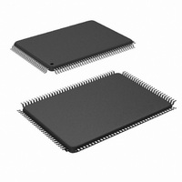
CLC5903VLA/NOPB National Semiconductor, CLC5903VLA/NOPB Datasheet - Page 18

CLC5903VLA/NOPB
Manufacturer Part Number
CLC5903VLA/NOPB
Description
IC DGTL TUNER/AGC DUAL 128-PQFP
Manufacturer
National Semiconductor
Type
Tunerr
Datasheet
1.CLC5903SMNOPB.pdf
(29 pages)
Specifications of CLC5903VLA/NOPB
Applications
Base Stations
Mounting Type
Surface Mount
Package / Case
128-MQFP, 128-PQFP
Lead Free Status / RoHS Status
Lead free / RoHS Compliant
Other names
*CLC5903VLA
*CLC5903VLA/NOPB
CLC5903VLA
*CLC5903VLA/NOPB
CLC5903VLA
Available stocks
Company
Part Number
Manufacturer
Quantity
Price
Company:
Part Number:
CLC5903VLA/NOPB
Manufacturer:
Texas Instruments
Quantity:
10 000
www.national.com
rate of 270.833kHz. An OSP starts when a sample is ready
and stops when the next one is ready.
Serial Outputs
The CLC5903 provides a serial clock (SCK), a frame strobe
(SFS) and two data lines (AOUT and BOUT) to output serial
data. The MUX_MODE control register specifies whether the
two channel outputs are transmitted on two separate serial
pins, or multiplexed onto one pin in a time division multi-
plexed (TDM) format. Separate output pins are not provided
for the I and Q halves of complex data. The I and Q outputs
are always multiplexed onto the same serial pin. The I-com-
ponent is output first, followed by the Q-component. By set-
ting the PACKED mode bit to ‘1’ a complex pair may be
treated as a single double-wide word. The RDY signal is
used to identify the first word of a complex pair of the TDM
formatted output when the SFS_MODE bit is set to ‘0’. Set-
ting SFS_MODE to ‘1’ causes the CLC5903 to output a sin-
gle SFS pulse for each output period. This SFS pulse will be
coincident with RDY and only a single SCK period wide. The
TDM modes are summarized in Table 1.
Output Modes
(b) PACKED MODE, ONE FRAME SYNC AT THE START OF EACH DOUBLE-WORD TRANSFER
A|BOUT
AOUT
AOUT
SCK
SFS
AOUT
SCK
SFS
AOUT
SCK
SFS
AOUT
RDY
SFS
SFS
SFS
Figure 30. Serial output formats. Refer to Figure 10 for detailed timing information
(c) ONE OR TWO CHANNEL MUX AND SFS MODES (PACKED MODE IS ON)
(a) UNPACKED MODE, FRAME SYNC AT THE START OF EACH WORD
(Continued)
leading edge of RDY aligns with leading edge of SFS
IA
IA
IA
QA
QA
QA
IB
IB
Output Sample Period (OSP)
mI7
I15
I15
clock stops and data is zero after transfers are complete
clock stops and data is zero after transfers are complete
mI6
QB
QB
clock stops and data is zero after transfers are complete
(d) FLOATING POINT FORMAT
I14
I14
MUX_MODE=0, SFS_MODE=0|1
MUX_MODE=1, SFS_MODE=0
MUX_MODE=1, SFS_MODE=1
mI0
eI3
I1
I1
18
eI2
The serial outputs use the format shown in Figure 30. Figure
30(a) shows the standard output mode (the PACKED mode
bit is low). The chip clocks the frame and data out of the chip
on the rising edge of SCK (or falling edge if the SCK_POL bit
in the input control register is set high). Data should be cap-
tured on the falling edge of SCK (rising if SCK_POL=1). The
I0
I0
SFS_MODE
eI0
0
1
Q15
Q15
eQ3
Q14
Q14
MUX_MODE
IA
IA
RDY is 2 CK periods wide
IA
Table 1. TDM Modes
0
1
0
1
eQ0
QA
QA
QA
Q1
Q1
mQ7
IB
IB
OUT
OUT
OUT
OUT
Q0
Q0
AOUT
SERIAL OUTPUTS
A
A
A
A
, OUT
, OUT
QB
QB
mQ0
B
B
OUT
LOW
OUT
LOW
BOUT
B
B


