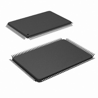
CLC5903VLA/NOPB National Semiconductor, CLC5903VLA/NOPB Datasheet - Page 2

CLC5903VLA/NOPB
Manufacturer Part Number
CLC5903VLA/NOPB
Description
IC DGTL TUNER/AGC DUAL 128-PQFP
Manufacturer
National Semiconductor
Type
Tunerr
Datasheet
1.CLC5903SMNOPB.pdf
(29 pages)
Specifications of CLC5903VLA/NOPB
Applications
Base Stations
Mounting Type
Surface Mount
Package / Case
128-MQFP, 128-PQFP
Lead Free Status / RoHS Status
Lead free / RoHS Compliant
Other names
*CLC5903VLA
*CLC5903VLA/NOPB
CLC5903VLA
*CLC5903VLA/NOPB
CLC5903VLA
Available stocks
Company
Part Number
Manufacturer
Quantity
Price
Company:
Part Number:
CLC5903VLA/NOPB
Manufacturer:
Texas Instruments
Quantity:
10 000
www.national.com
Functional Description
The CLC5903 block diagram is shown in Figure 2. The
CLC5903 contains two identical digital down-conversion
(DDC) circuits. Each DDC accepts an independently clocked
14-bit sample at up to 78MSPS, down converts from a
selected carrier frequency to baseband, decimates the signal
rate by a programmable factor ranging from 32 to 16384, pro-
vides channel filtering, and outputs quadrature symbols.
A crossbar switch enables either of the two inputs or a test
register to be routed to either DDC channel. Flexible channel
filtering is provided by the two programmable decimating FIR
filters. The final filter outputs can be converted to a 12-bit
floating point format or standard two’s complement format.
The output data is available at both serial and parallel ports.
The CLC5903 maintains over 100 dB of spurious free
dynamic range and over 100 dB of out-of-band rejection.
This allows considerable latitude in channel filter partitioning
between the analog and digital domains.
The frequencies, phase offsets, and phase dither of the two
sine/cosine numerically controlled oscillators (NCOs) can be
independently specified. Two sets of coefficient memories
and a crossbar switch allow shared or independent filter
coefficients and bandwidth for each channel. Both channels
share the same decimation ratio and input/output formats.
D[7:0]
A[7:0]
Input Source
CKA
CKB
TEST_REG
A_SOURCE
B_SOURCE
WR
AIN
BIN
RD
MR
CE
SI
Figure 2. CLC5903 Dual Digital Tuner / AGC Block Diagram with Control Register Associations
MUX
MUX
Microprocessor
Interface
A
B
CLK
GEN
Sync
Logic
14
14
DEC
DEC_BY_4
SCALE
EXP_INH
EXT_DELAY
Channel A
Tuning,
Channel Filters, and
AGC (see Figure 16)
Channel B
Tuning,
Channel Filters, and
AGC (see Figure 16)
Common Channel Controls
PHASE_A
PHASE_B
Channel A Controls
GAIN_A
Channel B Controls
GAIN_B
AGC_IC_A AGC_RB_A
AGC_IC_B AGC_RB_B
PAGE_SEL_F1
2
AGC_HOLD_IC
AGC_LOOP_GAIN
AGC_TABLE
AGC_COMB_ORD
FREQ_A
DITH_A
FREQ_B
DITH_B
Each channel has its own AGC circuit for use with narrow-
band radio channels where most of the channel filtering pre-
cedes the ADC. The AGC closes the loop around the
CLC5526 DVGA, compressing the dynamic range of the sig-
nal into the ADC. AGC gain compensation in the CLC5903
removes the DVGA gain steps at the output. The time align-
ment of this gain compensation circuit can be adjusted to
support ADCs with different latencies. The AGC can be con-
figured to operate continuously or set to a fixed gain step.
The two AGC circuits operate independently but share the
same programmed parameters and control signals.
The chip receives configuration and control information over
a microprocessor-compatible bus consisting of an 8-bit data
I/O port, an 8-bit address port, a chip enable strobe, a read
strobe, and a write strobe. The chip’s control registers (8 bits
each) are memory mapped into the 8-bit address space of
the control port. Page select bits allow access to the overlaid
A and B set of FIR coefficients.
JTAG boundary scan and on-chip diagnostic circuits are pro-
vided to simplify system debug and test.
The CLC5903 supports 3.3V I/O even though the core logic
voltage is 1.8V. The CLC5903 outputs swing to the 3.3V rail
so they can be directly connected to 5V TTL inputs if desired.
COEF_SEL_F1A
COEF_SEL_F2A
COEF_SEL_F1B
COEF_SEL_F2B
Output Formatter
Two’s Complement:
32-bit Truncated or
24-bit Rounded or
16-bit Rounded or
8-bit Truncated
(see Figure 29)
Floating Point:
4-bit Exponent and
8-bit Mantissa
or
F1A_COEFF
F1B_COEFF
PAGE_SEL_F2
F2A_COEFF
F2B_COEFF
Output Controls
SFS_MODE
RATE
SOUT_EN
SCK_POL
SFS_POL
RDY_POL
MUX_MODE
PACKED
FORMAT
DEBUG_EN
DEBUG_TAP
SDC_EN
AGAIN[2..0]
ASTROBE
SCK_IN
AOUT/BOUT
BOUT
SCK
SFS
RDY
POUT[15..0]
PSEL[2..0]
POUT_EN
BSTROBE
BGAIN[2..0]


