TFA9879 NXP Semiconductors, TFA9879 Datasheet - Page 25

TFA9879
Manufacturer Part Number
TFA9879
Description
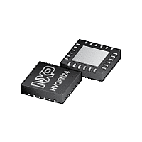
The TFA9879 contains a processor that supports a range of sound processing featuresincluding a 5-band parametric equalizer, separate bass and treble control, a dynamicrange compressor, soft clip control and volume control
Manufacturer
NXP Semiconductors
Datasheet
1.TFA9879.pdf
(60 pages)
Available stocks
Company
Part Number
Manufacturer
Quantity
Price
Company:
Part Number:
TFA9879HN/N1
Manufacturer:
ALTERA
Quantity:
332
Part Number:
TFA9879HN/N1,118
Manufacturer:
NXP/恩智浦
Quantity:
20 000
NXP Semiconductors
Table 18.
TFA9879
Product data sheet
Start
S
TFA9879
Address
11011A
I
2
C-bus write cycle
2
A
10.2 I
1
R/W
0
The TFA9879 is accessed via an 8-bit code (see
address. Bit 0 (R/W) indicates whether a read (1) or a write (0) operation has been
requested. Four separate addresses are supported for multichannel applications.
Applying the appropriate voltage to pins ADSEL1 (A1) and ADSEL2 (A2) select the
required I
Table 16.
Table 17.
The sequence of events that needs to be followed when writing data to the TFA9879’s
I
stores two bytes of data. Data is always written in byte pairs. Data transfer is always MSB
first.
The write cycle sequence using SDA is as follows:
10. The microcontroller can either assert the stop condition (P) or continue transmitting
Bit 7 (MSB) Bit 6
1
Logic value
0
1
2
2
1. The microcontroller asserts a start condition (S).
2. The microcontroller transmits the 7-bit device address of the TFA9879, followed by
3. The TFA9879 asserts an acknowledge (A).
4. The microcontroller transmits the 8-bit TFA9879 register address to which the first
5. The TFA9879 asserts an acknowledge.
6. The microcontroller transmits the first byte (the most significant byte).
7. The TFA9879 asserts an acknowledge.
8. The microcontroller transmits the second byte (the least significant byte).
9. The TFA9879 asserts an acknowledge.
C-bus registers is detailed in
C-bus write cycle
the R/W bit set to 0.
data byte will be written.
data by sending another pair of data bytes, repeating the sequence from step 6. In the
latter case, the targeted register address will have been auto-incremented by the
TFA9879.
A
2
C address as detailed in
I
I
2
2
TFA9879 first
register address
ADDR
C-bus device address
C pin voltages in I
1
All information provided in this document is subject to legal disclaimers.
Voltage on pins ADSEL1 and ADSEL2
< V
> V
IL
IH
Bit 5
0
Rev. 02 — 15 October 2010
2
A
C control mode
Table
Bit 4
1
Mono BTL class-D audio amplifier with digital input
Table
18. One byte is transmitted at a time. Each register
MSB
MS1
16.
Bit 3
1
A
Table
Bit 2
A2
16). Bits 1 to 7 contain the device
LSB
LS1
A
Bit 1
A1
TFA9879
© NXP B.V. 2010. All rights reserved.
More
data...
<....>
Bit 0 (LSB)
R/W
Stop
P
25 of 60


