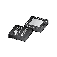
TFA9879 NXP Semiconductors, TFA9879 Datasheet - Page 6

TFA9879
Manufacturer Part Number
TFA9879
Description
The TFA9879 contains a processor that supports a range of sound processing featuresincluding a 5-band parametric equalizer, separate bass and treble control, a dynamicrange compressor, soft clip control and volume control
Manufacturer
NXP Semiconductors
Datasheet
1.TFA9879.pdf
(60 pages)
Available stocks
Company
Part Number
Manufacturer
Quantity
Price
Company:
Part Number:
TFA9879HN/N1
Manufacturer:
ALTERA
Quantity:
332
Part Number:
TFA9879HN/N1,118
Manufacturer:
NXP/恩智浦
Quantity:
20 000
NXP Semiconductors
9. Functional description
TFA9879
Product data sheet
Table 3.
The TFA9879 is a high-efficiency mono Bridge Tied Load (BTL) class-D amplifier with
digital audio inputs. It supports all commonly used formats.
The key functional blocks of the TFA9879 are shown in
audio signal is processed and converted into a Pulse Width Modulated (PWM) signal
using a 3-level modulation. In the analog domain, the PWM signal is amplified using a
second order feedback loop.
The audio signal-processing path is described below:
10. The H-BRIDGE allows the TFA9879 to deliver the required output power between
The internal clocks of the TFA9879 are derived from the digital audio interface (SCK1 and
SCK2) using a PLL. The reference input for the PLL is selected via the digital input MUX.
The audio signal path can be selected via the I
The PLL block generates the system clock.
Symbol
V
GNDD
DAP
1. The MUX selects the serial interface input to be used.
2. The digital audio receiver translates the serial input signal into a standard internal
3. The programmable high-pass filter blocks DC signals and low frequency signals.
4. The volume control provides both gain and attenuation functionality and can be
5. The 5-band parametric equalizer can be used to equalize the mono audio stream. It
6. The bass and treble boost function provides another way to adjust the sound.
7. The power limiter limits the maximum output signal of the TFA9879. The power limiter
8. The PWM controller block converts the audio signal into a 3-level modulated PWM
9. The second order feedback loop ensures excellent audio performance and high
DDD
mono audio stream.
adjusted by the user or dynamically via the Dynamic Range Compressor (DRC). The
volume control can be used to adjust the signal level between −70 dB and +24 dB.
can be used for speaker transfer curve compensation to optimize the audio
performance of the speakers.
settings are 0 dB to −124 dB in steps of 0.5 dB. This function can be used to limit the
maximum output power delivered to the speakers at a fixed supply voltage and
speaker impedance.
signal. The 3-level modulation provides a high signal-to-noise performance and
eliminates clock jitter noise.
power supply rejection ratio.
terminals OUTA and OUTB.
Pin
23
24
-
Pin description
All information provided in this document is subject to legal disclaimers.
Pin Type Description
P
P
P
Rev. 02 — 15 October 2010
…continued
digital supply voltage (1.8 V)
digital ground, PCB ground reference
exposed Die Attached Paddle (DAP); connect to PCB ground
Mono BTL class-D audio amplifier with digital input
2
C-bus interface.
Figure
1. In the digital domain, the
TFA9879
© NXP B.V. 2010. All rights reserved.
6 of 60


