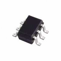
ADCMP601BKSZ-REEL7 Analog Devices Inc, ADCMP601BKSZ-REEL7 Datasheet - Page 6

ADCMP601BKSZ-REEL7
Manufacturer Part Number
ADCMP601BKSZ-REEL7
Description
IC COMP TTL/CMOS 1CHAN SC70-6
Manufacturer
Analog Devices Inc
Type
with Latchr
Specifications of ADCMP601BKSZ-REEL7
Number Of Elements
1
Output Type
CMOS, TTL
Voltage - Supply
2.5 V ~ 5.5 V
Mounting Type
Surface Mount
Package / Case
6-TSSOP, SC-88, SOT-363
Comparator Type
High Speed
No. Of Comparators
1
Response Time
3.5ns
Ic Output Type
CMOS, MOS, Open-Collector / Drain, TTL
Supply Current
3.5mA
Supply Voltage Range
2.5V To 5.5V
Rohs Compliant
Yes
Number Of Elements
1
Technology
CMOS
Input Offset Voltage
5mV
Input Bias Current (typ)
5uA
Single Supply Voltage (typ)
3/5V
Dual Supply Voltage (typ)
Not RequiredV
Supply Current (max)
4@5.5VmA
Power Supply Requirement
Single
Common Mode Rejection Ratio
50dB
Voltage Gain In Db
85dB
Power Supply Rejection Ratio
50dB
Single Supply Voltage (min)
2.5V
Single Supply Voltage (max)
5.5V
Dual Supply Voltage (min)
Not RequiredV
Dual Supply Voltage (max)
Not RequiredV
Power Dissipation
23mW
Operating Temp Range
-40C to 125C
Operating Temperature Classification
Automotive
Mounting
Surface Mount
Pin Count
6
Package Type
SC-70
Lead Free Status / RoHS Status
Lead free / RoHS Compliant
Other names
ADCMP601BKSZ-REEL7TR
Available stocks
Company
Part Number
Manufacturer
Quantity
Price
Part Number:
ADCMP601BKSZ-REEL7
Manufacturer:
ADI/亚德诺
Quantity:
20 000
ADCMP600/ADCMP601/ADCMP602
ABSOLUTE MAXIMUM RATINGS
Table 3.
Parameter
Supply Voltages
Input Voltages
Shutdown Control Pin
Latch/Hysteresis Control Pin
Output Current
Temperature
Input Supply Voltage (V
Output Supply Voltage
Positive Supply Differential
Input Voltage
Differential Input Voltage
Maximum Input/Output Current
Applied Voltage (HYS to GND)
Maximum Input/Output Current
Applied Voltage (HYS to GND)
Maximum Input/Output Current
Operating Temperature, Ambient
Operating Temperature, Junction
Storage Temperature Range
(V
(V
CCO
CCI
− V
to GND)
CCO
)
CCI
to GND)
−0.5 V to V
±(V
150°C
Rating
−0.5 V to +6.0 V
−0.5 V to +6.0 V
−6.0 V to +6.0 V
±50 mA
−0.5 V to V
±50 mA
−0.5 V to V
±50 mA
±50 mA
−40°C to +125°C
−65°C to +150°C
CCI
+ 0.5 V)
CCI
CCO
CCO
+ 0.5 V
+ 0.5 V
+ 0.5 V
Rev. A | Page 6 of 16
Stresses above those listed under Absolute Maximum Ratings
may cause permanent damage to the device. This is a stress
rating only; functional operation of the device at these or any
other conditions above those indicated in the operational
section of this specification is not implied. Exposure to absolute
maximum rating conditions for extended periods may affect
device reliability.
THERMAL RESISTANCE
θ
soldered in a circuit board for surface-mount packages.
Table 4. Thermal Resistance
Package Type
ADCMP600 SC70 5-Lead
ADCMP600 SOT-23 5-Lead
ADCMP601 SC70 6-Lead
ADCMP602 MSOP 5-Lead
1
ESD CAUTION
Measurement in still air.
JA
is specified for the worst-case conditions, that is, a device
θ
426
302
426
130
JA
1
Unit
°C/W
°C/W
°C/W
°C/W


