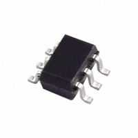
ADCMP601BKSZ-REEL7 Analog Devices Inc, ADCMP601BKSZ-REEL7 Datasheet - Page 7

ADCMP601BKSZ-REEL7
Manufacturer Part Number
ADCMP601BKSZ-REEL7
Description
IC COMP TTL/CMOS 1CHAN SC70-6
Manufacturer
Analog Devices Inc
Type
with Latchr
Specifications of ADCMP601BKSZ-REEL7
Number Of Elements
1
Output Type
CMOS, TTL
Voltage - Supply
2.5 V ~ 5.5 V
Mounting Type
Surface Mount
Package / Case
6-TSSOP, SC-88, SOT-363
Comparator Type
High Speed
No. Of Comparators
1
Response Time
3.5ns
Ic Output Type
CMOS, MOS, Open-Collector / Drain, TTL
Supply Current
3.5mA
Supply Voltage Range
2.5V To 5.5V
Rohs Compliant
Yes
Number Of Elements
1
Technology
CMOS
Input Offset Voltage
5mV
Input Bias Current (typ)
5uA
Single Supply Voltage (typ)
3/5V
Dual Supply Voltage (typ)
Not RequiredV
Supply Current (max)
4@5.5VmA
Power Supply Requirement
Single
Common Mode Rejection Ratio
50dB
Voltage Gain In Db
85dB
Power Supply Rejection Ratio
50dB
Single Supply Voltage (min)
2.5V
Single Supply Voltage (max)
5.5V
Dual Supply Voltage (min)
Not RequiredV
Dual Supply Voltage (max)
Not RequiredV
Power Dissipation
23mW
Operating Temp Range
-40C to 125C
Operating Temperature Classification
Automotive
Mounting
Surface Mount
Pin Count
6
Package Type
SC-70
Lead Free Status / RoHS Status
Lead free / RoHS Compliant
Other names
ADCMP601BKSZ-REEL7TR
Available stocks
Company
Part Number
Manufacturer
Quantity
Price
Part Number:
ADCMP601BKSZ-REEL7
Manufacturer:
ADI/亚德诺
Quantity:
20 000
PIN CONFIGURATION AND FUNCTION DESCRIPTIONS
Table 5. ADCMP600 (SOT-23-5 and SC70-5) Pin Function Descriptions
Pin No.
1
2
3
4
5
Table 6. ADCMP601 (SC70-6) Pin Function Descriptions
Pin No.
1
2
3
4
5
6
Table 7. ADCMP602 (MSOP-8) Pin Function Descriptions
Pin No.
1
2
3
4
5
6
7
8
Figure 3. ADCMP600 Pin Configuration
GND
V
Q
P
1
2
3
ADCMP600
(Not to Scale)
TOP VIEW
Mnemonic
Q
GND
V
V
V
Mnemonic
Q
GND
V
V
LE/HYS
V
Mnemonic
V
V
V
S
LE/HYS
GND
Q
V
DN
P
N
CCI
P
N
CCI
CCI
P
N
CCO
/V
/V
CCO
CCO
5
4
V
V
CCI
N
/V
CCO
Description
Noninverting Output. Q is at logic high if the analog voltage at the noninverting input, V
than the analog voltage at the inverting input, V
Negative Supply Voltage.
Noninverting Analog Input.
Inverting Analog Input.
Input Section Supply/Output Section Supply. Shared pin.
Description
Noninverting Output. Q is at logic high if the analog voltage at the noninverting input, V
than the analog voltage at the inverting input, V
Negative Supply Voltage.
Noninverting Analog Input.
Inverting Analog Input.
Latch/Hysteresis Control. Bias with resistor or current for hysteresis adjustment; drive low to latch.
Input Section Supply/Output Section Supply. Shared pin.
Description
Input Section Supply.
Noninverting Analog Input.
Inverting Analog Input.
Shutdown. Drive this pin low to shut down the device.
Latch/Hysteresis Control. Bias with resistor or current for hysteresis adjustment; drive low to latch.
Negative Supply Voltage.
Noninverting Output. Q is at logic high if the analog voltage at the noninverting input, V
than the analog voltage at the inverting input, V
Output Section Supply.
Figure 4. ADCMP601 Pin Configuration
GND
V
Q
P
1
2
3
ADCMP601
(Not to Scale)
Rev. A | Page 7 of 16
TOP VIEW
6
5
4
V
LE/HYS
V
CCI
N
/V
CCO
N
N
N
ADCMP600/ADCMP601/ADCMP602
.
, if the comparator is in compare mode.
, if the comparator is in compare mode.
Figure 5. ADCMP602 Pin Configuration
V
S
CCI
V
V
DN
N
P
1
2
3
4
ADCMP602
(Not to Scale)
TOP VIEW
8
7
6
5
P
P
P
, is greater
, is greater
, is greater
V
Q
GND
LE/HYS
CCO


