NUP1301U NXP Semiconductors, NUP1301U Datasheet - Page 8

NUP1301U
Manufacturer Part Number
NUP1301U
Description
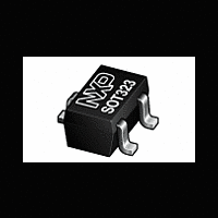
Ultra low capacitance ElectroStatic Discharge (ESD) protection array in a smallSOT323 (SC-70) Surface-Mounted Device (SMD) plastic package designed toprotect one signal line in rail-to-rail configuration from the damage caused byESD and other transie
Manufacturer
NXP Semiconductors
Datasheet
1.NUP1301U.pdf
(14 pages)
Available stocks
Company
Part Number
Manufacturer
Quantity
Price
Part Number:
NUP1301U
Manufacturer:
NXP
Quantity:
20 000
NXP Semiconductors
8. Application information
9. Test information
NUP1301U
Product data sheet
9.1 Quality information
Protection of a single (high-speed) data line in rail-to-rail configuration. The protected data
line is connected to pin 3. Pin 1 is connected to ground (GND) and pin 2 is connected to
the supply rail (supply voltage V
voltage drop of one diode, the transient is directed either to the supply rail or to GND.
The advantages of these solutions are: low line capacitance (0.6 pF typically), fast
response time, and low clamping voltage.
Circuit board layout and protection device placement:
Circuit board layout is critical for the suppression of ESD, Electrical Fast Transient (EFT)
and surge transients. The following guidelines are recommended:
This product has been qualified in accordance with the Automotive Electronics Council
(AEC) standard Q101 - Stress test qualification for discrete semiconductors, and is
suitable for use in automotive applications.
1. Place the NUP1301U as close to the input terminal or connector as possible.
2. The path length between the NUP1301U and the protected line should be minimized.
3. Keep parallel signal paths to a minimum.
4. Avoid running protected conductors in parallel with unprotected conductors.
5. Minimize all Printed-Circuit Board (PCB) conductive loops including power and
6. Minimize the length of the transient return path to ground.
7. Avoid using shared transient return paths to a common ground point.
8. Ground planes should be used whenever possible. For multilayer PCBs, use ground
Fig 8.
ground loops.
vias.
Typical application for the protection of one signal line
All information provided in this document is subject to legal disclaimers.
Rev. 1 — 28 January 2011
interface
Audio
CC
). When the transient voltage exceeds the forward
V
CC
Ultra low capacitance ESD protection array
D1
NUP1301U
V
CC
D2
NUP1301U
006aac518
NUP1301U
© NXP B.V. 2011. All rights reserved.
8 of 14


