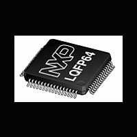
LPC1227FBD64 NXP Semiconductors, LPC1227FBD64 Datasheet - Page 14

LPC1227FBD64
Manufacturer Part Number
LPC1227FBD64
Description
The LPC1227FBD64 is an ARM Cortex-M0 based microcontroller for embedded applications featuring a high level of integration and low power consumption
Manufacturer
NXP Semiconductors
Datasheet
1.LPC1224FBD48.pdf
(61 pages)
Available stocks
Company
Part Number
Manufacturer
Quantity
Price
Company:
Part Number:
LPC1227FBD64
Manufacturer:
AD
Quantity:
31
Part Number:
LPC1227FBD64
Manufacturer:
NXP/恩智浦
Quantity:
20 000
Company:
Part Number:
LPC1227FBD64/301
Manufacturer:
NXP
Quantity:
5 000
Company:
Part Number:
LPC1227FBD64/301
Manufacturer:
NXP
Quantity:
5 000
Part Number:
LPC1227FBD64/301
Manufacturer:
NXP/恩智浦
Quantity:
20 000
Company:
Part Number:
LPC1227FBD64/301,1
Manufacturer:
NXP Semiconductors
Quantity:
10 000
NXP Semiconductors
Table 3.
[1]
[2]
[3]
[4]
[5]
[6]
[7]
[8]
[9]
[10] If the RTC is not used, RTCXIN and RTCXOUT can be left floating.
LPC122X
Product data sheet
Symbol
V
V
V
V
DD(IO)
DD(3V3)
SSIO
SS
Pin state at reset for default function: I = Input; O = Output; PU = internal pull-up enabled; IA = inactive, no pull-up/down enabled.
3.3 V tolerant, digital I/O pin; default: pull-up enabled, no hysteresis.
If set to output, this normal-drive pin is in low mode by default.
I
3.3 V tolerant, digital I/O pin with RESET function; default: pull-up enabled, no hysteresis. An external pull-up resistor is required on this
pin for the Deep power-down mode.
3.3 V tolerant, digital I/O pin with analog function; default: pull-up enabled, no hysteresis.
If set to output, this normal-drive pin is in high mode by default.
3.3 V tolerant, digital I/O pin with analog function and WAKEUP function; default: pull-up enabled, no hysteresis.
3.3 V tolerant, high-drive digital I/O pin; default: pull-up enabled, no hysteresis.
2
C-bus pins; 5 V tolerant; open-drain; default: no pull-up/pull-down; no hysteresis.
LPC122x pin description
To enable a peripheral function, find the corresponding port pin, or select a port pin if the
function is multiplexed, and program the port pin’s IOCONFIG register to enable that
function. The primary SWD functions and RESET are the default functions on their pins
after reset.
Table 4.
Peripheral
Analog comparators
47 63
44 56
48 64
43 55
Pin multiplexing
Start
logic
input
-
-
-
-
…continued
All information provided in this document is subject to legal disclaimers.
Type Reset
I
I
I
I
Rev. 2 — 26 August 2011
Function
ROSC
ACMP0_I0
ACMP0_I1
ACMP0_I2
ACMP0_I3
ACMP0_O
ACMP1_I0
ACMP1_I1
ACMP1_I2
ACMP1_I3
ACMP1_O
state
[1]
-
-
-
-
Description
Input/output supply voltage.
3.3 V supply voltage to the internal regulator and the ADC. Also
used as the ADC reference voltage.
Ground.
Ground.
Type
I/O
I
I
I
I
O
I
I
I
I
O
32-bit ARM Cortex-M0 microcontroller
Available on ports:
PIO0_29
PIO0_19
PIO0_20
PIO0_21
PIO0_22
PIO0_27
PIO0_23
PIO0_24
PIO0_25
PIO0_26
PIO0_28
-
-
-
-
-
-
-
-
-
-
-
LPC122x
© NXP B.V. 2011. All rights reserved.
-
-
-
-
-
-
-
-
-
-
-
14 of 61


