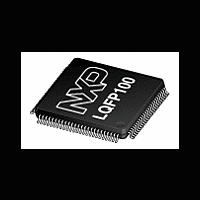
LPC2921_23_25 NXP Semiconductors, LPC2921_23_25 Datasheet - Page 44

LPC2921_23_25
Manufacturer Part Number
LPC2921_23_25
Description
The LPC2921/2923/2925 combine an ARM968E-S CPU core with two integrated TCMblocks operating at frequencies of up to 125 MHz, Full-speed USB 2
Manufacturer
NXP Semiconductors
Datasheet
1.LPC2921_23_25.pdf
(84 pages)
- Current page: 44 of 84
- Download datasheet (552Kb)
NXP Semiconductors
LPC2921_23_25_3
Product data sheet
Configuration of the CGU0:
choice can be made from the primary and secondary clock generators according to
Figure
Any output generator (except for BASE_SAFE_CLK and BASE_PCR_CLK) can be
connected to either a fractional divider (FDIV[0:6]) or to one of the outputs of the PLL or to
LP_OSC/crystal oscillator directly. BASE_SAFE_CLK and BASE_PCR_CLK can use only
LP_OSC as source.
The fractional dividers can be connected to one of the outputs of the PLL or directly to
LP_OSC/crystal Oscillator.
The PLL is connected to the crystal oscillator.
In this way every output generating the base clocks can be configured to get the required
clock. Multiple output generators can be connected to the same primary or secondary
clock source, and multiple secondary clock sources can be connected to the same PLL
output or primary clock source.
Invalid selections/programming - connecting the PLL to an FDIV or to one of the PLL
outputs itself for example - will be blocked by hardware. The control register will not be
written, the previous value will be kept, although all other fields will be written with new
data. This prevents clocks being blocked by incorrect programming.
Default Clock Sources:
connected to LP_OSC at reset. In this way the device runs at a low frequency after reset.
It is recommended to switch BASE_SYS_CLK to a high-frequency clock generator as
(one of) the first step(s) in the boot code after verifying that the high-frequency clock
generator is running.
Clock Activity Detection:
and values of ‘CLK_SEL’ that would select those clocks are masked and not written to the
control registers. This is accomplished by adding a clock detector to every clock
Fig 10. Structure of the clock generation scheme
10.
OSCILLATOR
EXTERNAL
All information provided in this document is subject to legal disclaimers.
LP_OSC
Rev. 03 — 14 April 2010
Every secondary clock generator or output generator is
Clocks that are inactive are automatically regarded as invalid,
For every output generator generating the base clocks a
PLL
ARM9 microcontroller with CAN, LIN, and USB
clkout
clkout120
clkout240
LPC2921/2923/2925
CONTROL
OUTPUT
outputs
clock
© NXP B.V. 2010. All rights reserved.
FDIV0:6
002aad834
44 of 84
Related parts for LPC2921_23_25
Image
Part Number
Description
Manufacturer
Datasheet
Request
R
Part Number:
Description:
Arm9 Microcontroller With Can, Lin, And Usb Device
Manufacturer:
NXP Semiconductors
Datasheet:
Part Number:
Description:
(LPC2921 - LPC2925) ARM9 microcontroller
Manufacturer:
NXP Semiconductors
Datasheet:
Part Number:
Description:
NXP Semiconductors designed the LPC2420/2460 microcontroller around a 16-bit/32-bitARM7TDMI-S CPU core with real-time debug interfaces that include both JTAG andembedded trace
Manufacturer:
NXP Semiconductors
Datasheet:

Part Number:
Description:
NXP Semiconductors designed the LPC2458 microcontroller around a 16-bit/32-bitARM7TDMI-S CPU core with real-time debug interfaces that include both JTAG andembedded trace
Manufacturer:
NXP Semiconductors
Datasheet:
Part Number:
Description:
NXP Semiconductors designed the LPC2468 microcontroller around a 16-bit/32-bitARM7TDMI-S CPU core with real-time debug interfaces that include both JTAG andembedded trace
Manufacturer:
NXP Semiconductors
Datasheet:
Part Number:
Description:
NXP Semiconductors designed the LPC2470 microcontroller, powered by theARM7TDMI-S core, to be a highly integrated microcontroller for a wide range ofapplications that require advanced communications and high quality graphic displays
Manufacturer:
NXP Semiconductors
Datasheet:
Part Number:
Description:
NXP Semiconductors designed the LPC2478 microcontroller, powered by theARM7TDMI-S core, to be a highly integrated microcontroller for a wide range ofapplications that require advanced communications and high quality graphic displays
Manufacturer:
NXP Semiconductors
Datasheet:
Part Number:
Description:
The Philips Semiconductors XA (eXtended Architecture) family of 16-bit single-chip microcontrollers is powerful enough to easily handle the requirements of high performance embedded applications, yet inexpensive enough to compete in the market for hi
Manufacturer:
NXP Semiconductors
Datasheet:
Part Number:
Description:
The XA-S3 device is a member of Philips Semiconductors? XA(eXtended Architecture) family of high performance 16-bitsingle-chip microcontrollers
Manufacturer:
NXP Semiconductors
Datasheet:

Part Number:
Description:
The NXP BlueStreak LH75401/LH75411 family consists of two low-cost 16/32-bit System-on-Chip (SoC) devices
Manufacturer:
NXP Semiconductors
Datasheet:

Part Number:
Description:
The NXP LPC3130/3131 combine an 180 MHz ARM926EJ-S CPU core, high-speed USB2
Manufacturer:
NXP Semiconductors
Datasheet:

Part Number:
Description:
The NXP LPC3141 combine a 270 MHz ARM926EJ-S CPU core, High-speed USB 2
Manufacturer:
NXP Semiconductors

Part Number:
Description:
The NXP LPC3143 combine a 270 MHz ARM926EJ-S CPU core, High-speed USB 2
Manufacturer:
NXP Semiconductors

Part Number:
Description:
The NXP LPC3152 combines an 180 MHz ARM926EJ-S CPU core, High-speed USB 2
Manufacturer:
NXP Semiconductors


