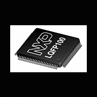
XA-H4 NXP Semiconductors, XA-H4 Datasheet - Page 29

XA-H4
Manufacturer Part Number
XA-H4
Description
The powerful 16-bit XA CPU core and rich feature set make the XA-H3 and XA-H4 devices ideal for high-performance real-time applications such as industrial control and networking
Manufacturer
NXP Semiconductors
Datasheet
1.XA-H4.pdf
(42 pages)
1. See notes after the 3.3 V AC Timing Table
Philips Semiconductors
PRELIMINARY AC ELECTRICAL CHARACTERISTICS (5.0 V +/–10%)
V
NOTE:
1999 Sep 24
DD
Symbol
Symbol
t
t
t
t
t
t
t
t
t
t
t
t
t
t
t
t
Single-chip 16-bit microcontroller
t
t
t
CODH
CPWH
CHCX
CHAH
CHSH
CPWL
AHDR
OHDE
CHDV
SHAH
SHDH
CLCX
CLCH
CHCL
CHAV
CHSL
DVSL
CLRL
AVSL
t
t
t
t
t
F
DIS
DIH
WS
WH
t
RP
= 5.0 V +/– 10%; T
C
C
7, 8, 10, 11, 12, 14, 15,
7, 8, 10, 14, 15, 17, 18
11, 12, 17, 18, 19, 20
8, 10, 11, 14, 18
17, 18, 19
Fig re
Figure
11, 19
16, 20
7, 14
9, 13
9, 16
9, 16
amb
23
23
23
23
23
All
All
All
All
All
24
22
21
25
25
= –40 C to +85 C (industrial)
System Clock Frequency
System Clock Period = 1/FC
XTALIN High Time
XTALIN Low Time
XTALIN Rise Time
XTALIN Fall Time
Address Valid to Strobe low
Address hold after ClkOut rising edge
Delay from ClkOut rising edge to address valid
Delay from ClkOut rising edge to Strobe High
Delay from ClkOut rising edge to Strobe Low
ClkOut Duty Cycle High (into 40 pF max.)
CAS Pulse Width High
CAS Pulse Width Low
RAS precharge time, thus minimum RAS high time
Address hold (A19 – A1 only, not A0) after CS, BLE, BHE rise at
end of Generic Data Read Cycle (not code fetch)
Data In Valid setup to ClkOut rising edge
Data In Valid hold after ClkOut rising edge
OE high to XA Data Bus Driver Enable
Clock High to Data Valid
Data Valid prior to Strobe Low
Minimum Address Hold Time after strobe goes inactive
Data hold after strobes (CS and BHE/BLE) high
CAS low to RAS low
WAIT setup (stable high or low) to ClkOut rising edge
WAIT hold (stable high or low) after ClkOut rising edge
Data Read and Instruction Fetch Cycles
Generic Data Read Only
All DRAM Cycles
Write Cycles
All Cycles
Wait Input
Parameter
Parameter
Refresh
29
9
2
9
9
8
(n * t
t
t
t
t
t
t
t
t
t
t
t
t
CHCX
33.33
C
C
C
C
C
C
C
C
C
C
C
Min
C
* 0.5
* 0.4
25
20
– 21
– 12
– 10
– 12
– 14
– 23
– 25
– 25
– 15
0
–
–
1
–
1
1
0
–
0
) – 16
–7
Limits
8
Preliminary specification
t
CHCX
Max
30
25
21
19
25
–
–
–
5
5
–
–
–
–
–
–
–
–
–
–
–
–
–
–
–
XA-H4
+3
MHz
Unit
Unit
ns
ns
ns
ns
ns
ns
ns
ns
ns
ns
ns
ns
ns
ns
ns
ns
ns
ns
ns
ns
ns
ns
ns
ns
ns


