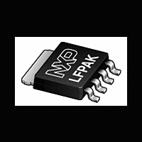
PSMN3R5-30YL NXP Semiconductors, PSMN3R5-30YL Datasheet - Page 6

PSMN3R5-30YL
Manufacturer Part Number
PSMN3R5-30YL
Description
Logic level N-channel enhancement mode Field-Effect Transistor (FET) in a plastic package using TrenchMOS technology
Manufacturer
NXP Semiconductors
Datasheet
1.PSMN3R5-30YL.pdf
(14 pages)
Available stocks
Company
Part Number
Manufacturer
Quantity
Price
Company:
Part Number:
PSMN3R5-30YL
Manufacturer:
NXP
Quantity:
51 000
Part Number:
PSMN3R5-30YL
Manufacturer:
NEXPERIA/安世
Quantity:
20 000
Part Number:
PSMN3R5-30YL,115
Manufacturer:
NXP/恩智浦
Quantity:
20 000
NXP Semiconductors
Table 6.
Tested to JEDEC standards where applicable.
PSMN3R5-30YL
Product data sheet
Symbol
Source-drain diode
V
t
Q
rr
Fig 5.
Fig 7.
SD
r
R
(mΩ)
DSon
(A)
I
80
60
40
20
D
0
6
4
2
function of gate-source voltage; typical values
of gate-source voltage; typical values
Transfer characteristics: drain current as a
Drain-source on-state resistance as a function
0
2
Characteristics
Parameter
source-drain voltage
reverse recovery time
recovered charge
1
4
T
j
= 150 °C
…continued
2
6
25 °C
8
3
Conditions
I
see
I
V
All information provided in this document is subject to legal disclaimers.
S
S
V
V
DS
003aac711
003aac709
= 25 A; V
= 20 A; dI
GS
GS
Figure 17
= 20 V
(V)
(V)
10
4
Rev. 4 — 9 March 2011
GS
S
/dt = -100 A/µs; V
= 0 V; T
N-channel 30 V 3.5 mΩ logic level MOSFET in LFPAK
Fig 6.
Fig 8.
j
= 25 °C;
4000
3000
2000
1000
(pF)
100
(A)
I
80
60
40
20
C
D
0
0
function of drain-source voltage; typical values
function of gate-source voltage; typical values
Output characteristics: drain current as a
Input and reverse transfer capacitances as a
GS
0
0
C
V
= 0 V;
C
rss
GS
iss
10
(V) = 4.5
2
2
PSMN3R5-30YL
4
4
Min
-
-
-
6
6
Typ
0.82
37
31
© NXP B.V. 2011. All rights reserved.
8
8
003aac710
003aac716
V
V
GS
DS
Max
1.2
-
-
2.6
2.4
(V)
2.2
(V)
2.8
3
10
10
Unit
V
ns
nC
6 of 14


