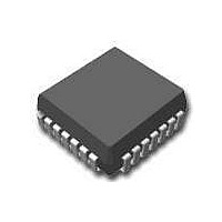
MC10E1652FNG ON Semiconductor, MC10E1652FNG Datasheet - Page 4

MC10E1652FNG
Manufacturer Part Number
MC10E1652FNG
Description
IC COMPARATOR DUAL ECL 20PLCC
Manufacturer
ON Semiconductor
Series
MOSAIC III™r
Type
with Latchr
Datasheet
1.MC10E1652FNR2G.pdf
(10 pages)
Specifications of MC10E1652FNG
Number Of Elements
2
Output Type
Differential, ECL
Mounting Type
Surface Mount
Package / Case
20-LCC (J-Lead)
Number Of Channels
2 Channels
Product
Analog Comparators
Response Time
475 ps
Supply Voltage (max)
5 V
Supply Voltage (min)
- 5.2 V
Supply Current (max)
50 mA
Maximum Operating Temperature
+ 85 C
Mounting Style
SMD/SMT
High Level Output Current
150 uA
Minimum Operating Temperature
0 C
Propagation Delay Time
925 ps
Lead Free Status / RoHS Status
Lead free / RoHS Compliant
Other names
MC10E1652FNGOS
Available stocks
Company
Part Number
Manufacturer
Quantity
Price
Company:
Part Number:
MC10E1652FNG
Manufacturer:
ON Semiconductor
Quantity:
135
Company:
Part Number:
MC10E1652FNG
Manufacturer:
ON Semiconductor
Quantity:
10 000
NOTE: Device will meet the specifications after thermal equilibrium has been established when mounted in a test socket or printed circuit
6. Input V
7. The propagation delay is measured from the crosspoint of the input signal and the threshold value to the crosspoint of the Q and Q output
8. t
9. Refer to Figure 4 and note that the input is at 850 mV ECL levels with the input threshold range between the 20% and 80% points. The delay
10. The slew rate is 0.25 V/NS for input rising edges.
11. The slew rate is 0.75 V/NS for input rising edges.
12. Refer to Figure 5 and note that the input is at 2.5 V TTL levels with the input threshold range between the 20% and 80% points. The delay
13. The slew rate is 0.3 V/NS for input rising edges.
Table 5. AC CHARACTERISTICS
Symbol
f
t
t
t
t
t
t
t
T
T
VPP
t
t
MAX
PLH
PHL
s
h
pw
skew
JITTER
r
f
DE
DL
signals. For propagation delay measurements the threshold level (V
0.75 V/NS. There is an insignificant change in the propagation delay over the input common mode range.
is measured from the crosspoint of the input signal and the threshold value to the crosspoint of the Q and Q output signals.
is measured from the crosspoint of the input signal and the threshold value to the crosspoint of the Q and Q output signals.
skew
board with maintained transverse airflow greater than 500 lfpm. Electrical parameters are guaranteed only over the declared
operating temperature range. Functional operation of the device exceeding these conditions is not implied. Device specification limit
values are applied individually under normal operating conditions and not valid simultaneously.
is the propagation delay skew between comparator A and comparator B for a particular part under identical input conditions.
−0.8
−1.0
−1.2
−1.4
−1.6
−1.8
IL
Maximum Toggle Frequency
Propagation Delay to Output (Note 7)
Setup Time
Enable Hold Time
Minimum Pulse Width
Within Device Skew (Note 8)
Cycle−to−Cycle Jitter
Delay Dispersion
Delay Dispersion
Differential Input Voltage
Rise/Fall Times
Figure 3. Typical Hysteresis Curve
and V
−20 −16 −12 −8
(20-80%)
IH
Vin, DIFFERENTIAL INPUT VOLTAGE (mV)
parameters vary 1:1 with V
Characteristic
(TTL Levels) (Notes 12, 13)
(ECL Levels) (Notes 9 10)
HYSTERESIS
−4 Vref
V
|V1 − V2|
CC
4
(Notes 11, 12)
(Notes 9, 11)
= +5.0 V ±5%; V
8
LEN to Q
CC
V to Q
. Output V
12
LEN
V
V
16
http://onsemi.com
Min
750
550
450
−50
400
225
20
OH
EE
and V
= −5.2 V ±5%, V
−250
TBD
TBD
0°C
Typ
900
725
300
325
4
15
OL
THR
parameters vary 1:1 with GND.
) is centered about an 850 mV input logic swing with a slew rate of
1050
Max
900
475
3.7
CC
40
30
20
10
0
−0.2
Min
= 0 V (Note 6)
775
550
450
−50
400
225
PROGRAMMING VOLTAGE (VOLTAGE ABOVE VEE)
Figure 4. Hysteresis Programming Voltage
25°C
T =
−0.1
25°C
> 1.0
−250
TBD
Typ
925
750
300
100
350
100
325
15
60
T = 0°C
0.0
1075
Max
900
475
3.7
0.1
−100
0.2
Min
850
650
550
400
250
85°C
0.3
T =
1025
−250
85°C
TBD
TBD
Typ
825
350
375
15
0.4
1200
1000
Max
500
3.7
0.5
Unit
GHz
ps
ps
ps
ps
ps
ps
ps
ps
ps
V


