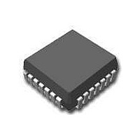
MC10E1652FNG ON Semiconductor, MC10E1652FNG Datasheet - Page 5

MC10E1652FNG
Manufacturer Part Number
MC10E1652FNG
Description
IC COMPARATOR DUAL ECL 20PLCC
Manufacturer
ON Semiconductor
Series
MOSAIC III™r
Type
with Latchr
Datasheet
1.MC10E1652FNR2G.pdf
(10 pages)
Specifications of MC10E1652FNG
Number Of Elements
2
Output Type
Differential, ECL
Mounting Type
Surface Mount
Package / Case
20-LCC (J-Lead)
Number Of Channels
2 Channels
Product
Analog Comparators
Response Time
475 ps
Supply Voltage (max)
5 V
Supply Voltage (min)
- 5.2 V
Supply Current (max)
50 mA
Maximum Operating Temperature
+ 85 C
Mounting Style
SMD/SMT
High Level Output Current
150 uA
Minimum Operating Temperature
0 C
Propagation Delay Time
925 ps
Lead Free Status / RoHS Status
Lead free / RoHS Compliant
Other names
MC10E1652FNGOS
Available stocks
Company
Part Number
Manufacturer
Quantity
Price
Company:
Part Number:
MC10E1652FNG
Manufacturer:
ON Semiconductor
Quantity:
135
Company:
Part Number:
MC10E1652FNG
Manufacturer:
ON Semiconductor
Quantity:
10 000
the MC10E1652’s compare and latch features. When the
signal on the LEN pin is at a logic high level, the device is
operating in the “compare mode,” and the signal on the input
arrives at the output after a nominal propagation delay (t
t
to the negative going transition on LEN and held for a time,
t
operating in the “latch mode,” thus transitions on the input
do not appear at the output. The device continues to operate
in the “latch mode” until the latch is asserted once again.
Moreover, the LEN pulse must meet the minimum pulse
width (t
relationship. Note that the LEN waveform in Figure 5.
shows the LEN signal swinging around a reference labeled
VBB
LEN follow typical ECL 10KH logic levels because
PLH
h
, after the LEN transition. After time t
VBB
The timing diagram (Figure 5.) is presented to illustrate
V
LEN
). The input signal must be asserted for a time, t
THR
INT
INT
Q
Q
V
pw
; this waveform emphasizes the requirement that
) requirement to effect the correct input-output
V
IN
t
s
V
OD
Figure 5. Input/Output Timing Diagram
t
t
PHL
h
APPLICATIONS INFORMATION
h
, the latch is
s
http://onsemi.com
, prior
PHL
,
5
VBB
nominally at the ECL VBB level.
the voltage level beyond the threshold level (V
the input is driven. As an example, if the threshold level is
set on one of the comparator inputs as 80 mV and the input
signal swing on the complementary input is from zero to 100
mV, the positive going overdrive would be 20 mV and the
negative going overdrive would be 80 mV. The result of
differing overdrive levels is that the devices have shorter
propagation delays with greater overdrive because the
threshold level is crossed sooner than the case of lower
overdrive levels. Typically, semiconductor manufactures
refer to the threshold voltage as the input offset voltage
(VOS) since the threshold voltage is the sum of the
externally supplied reference voltage and inherent device
offset voltage.
Finally, V
INT
is the internally generated reference level, hence is
OD
is the input voltage overdrive and represents
t
pw
t
PLH(LEN)
THR
) to which


